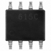
BSO615CT Infineon Technologies, BSO615CT Datasheet

BSO615CT
Specifications of BSO615CT
Related parts for BSO615CT
BSO615CT Summary of contents
Page 1
SIPMOS Small-Signal-Transistor Features Dual N- and P -Channel Enhancement mode Logic Level Avalanche rated rated Type Package BSO 615 Maximum Ratings, °C, unless otherwise specified j Parameter Continuous drain current ...
Page 2
Termal Characteristics Parameter Dynamic Characteristics Thermal resistance, junction - soldering point ( Pin 4) SMD version, device on PCB: @ min. footprint sec cooling area ; t @ min. footprint sec. ...
Page 3
Electrical Characteristics Parameter Characteristics Transconductance DS(on)max DS(on)max Input capacitance ...
Page 4
Electrical Characteristics Parameter Characteristics Gate to source charge 3 - Gate to drain charge ...
Page 5
Power Dissipation (N-Ch tot A BSO 615 C 2.2 W 1.8 1.6 1.4 1.2 1.0 0.8 0.6 0.4 0.2 0 Drain current (N-Ch ...
Page 6
Safe operating area (N-Ch parameter : °C A BSO 615 ...
Page 7
Typ. output characteristics (N-Ch parameter µs p BSO 615 C 7 2.00W tot 6.0 5.5 5.0 4.5 4.0 3.5 3.0 2.5 2.0 1.5 1.0 ...
Page 8
Typ. transfer characteristics (N-Ch.) parameter µ 7.0 A 6.0 5.5 5.0 4.5 4.0 3.5 3.0 2.5 2.0 1.5 1.0 0.5 ...
Page 9
Drain-source on-resistance (N-Ch DS(on) j parameter : BSO 615 C 0.30 0.24 0.22 0.20 0.18 0.16 98% 0.14 0.12 0.10 typ 0.08 0.06 0.04 0.02 0.00 ...
Page 10
Typ. capacitances (N-Ch parameter MHz Forward characteristics of reverse diode (N-Ch.) ...
Page 11
Avalanche Energy parameter 3 105 Typ. gate charge ...
Page 12
Drain-source breakdown voltage (N-Ch.) (BR)DSS j BSO 615 -60 - Preliminary data Drain-source breakdown voltage V (BR)DSS -72 V -68 -66 ...
Page 13
... For information on the types in question please contact your nearest Infineon Technologies Office. Infineon Technologies Components may only be used in life-support devices or systems with the express written approval of Infineon Technologies failure of such components can reasonably be expected to cause the failure of that life-support device or system affect the safety or effectiveness of that device or system Life support devices or systems are intended to be implanted in the human body support and/or maintain and sustain and/or protect human life ...


