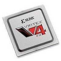
XC4VFX20-10FFG672C Xilinx Inc, XC4VFX20-10FFG672C Datasheet - Page 60

XC4VFX20-10FFG672C
Manufacturer Part Number
XC4VFX20-10FFG672C
Description
IC FPGA VIRTEX-4 FX 20K 672-FBGA
Manufacturer
Xilinx Inc
Series
Virtex™-4r
Datasheets
1.XC4VFX12-10FFG668C.pdf
(58 pages)
2.XC4VFX12-10FFG668C.pdf
(9 pages)
3.XC4VFX12-10FFG668C.pdf
(406 pages)
Specifications of XC4VFX20-10FFG672C
Total Ram Bits
1253376
Number Of Logic Elements/cells
19224
Number Of Labs/clbs
2136
Number Of I /o
320
Voltage - Supply
1.14 V ~ 1.26 V
Mounting Type
Surface Mount
Operating Temperature
0°C ~ 85°C
Package / Case
672-BBGA, FCBGA
No. Of Logic Blocks
19224
No. Of Macrocells
19224
No. Of Speed Grades
10
No. Of I/o's
320
Clock Management
DCM
I/o Supply Voltage
3.45V
Lead Free Status / RoHS Status
Lead free / RoHS Compliant
For Use With
HW-V4-ML405-UNI-G - EVALUATION PLATFORM VIRTEX-4
Number Of Gates
-
Lead Free Status / RoHS Status
Lead free / RoHS Compliant, Lead free / RoHS Compliant
Available stocks
Company
Part Number
Manufacturer
Quantity
Price
Company:
Part Number:
XC4VFX20-10FFG672C
Manufacturer:
ADVANTEK
Quantity:
314
Company:
Part Number:
XC4VFX20-10FFG672C
Manufacturer:
XilinxInc
Quantity:
3 000
Company:
Part Number:
XC4VFX20-10FFG672C
Manufacturer:
Xilinx Inc
Quantity:
10 000
Part Number:
XC4VFX20-10FFG672C
Manufacturer:
XILINX/赛灵思
Quantity:
20 000
- XC4VFX12-10FFG668C PDF datasheet
- XC4VFX12-10FFG668C PDF datasheet #2
- XC4VFX12-10FFG668C PDF datasheet #3
- Current page: 60 of 406
- Download datasheet (6Mb)
Chapter 2: Digital Clock Managers (DCMs)
60
Phase-Shift Clock Input — PSCLK
Dynamic Reconfiguration Clock Input — DCLK
1.
2.
3.
The phase-shift clock (PSCLK) input pin provides the source clock for the DCM phase
shift. The PSCLK can be asynchronous (in phase and frequency) to CLKIN. The phase-shift
clock signal can be driven by any clock source (external or internal), including:
1.
2.
3.
4.
The frequency range of PSCLK is defined by PSCLK_FREQ_LF/HF (see the
Sheet). This input must be tied to ground when the CLKOUT_PHASE_SHIFT attribute is
set to NONE or FIXED.
The dynamic reconfiguration clock (DCLK) input pin provides the source clock for the
DCM's dynamic reconfiguration circuit. The frequency of DCLK can be asynchronous (in
phase and frequency) to CLKIN. The dynamic reconfiguration clock signal is driven by
any clock source (external or internal), including:
1.
2.
3.
4.
The frequency range of DCLK is described in the
reconfiguration is not used, this input must be tied to ground. See the dynamic
reconfiguration chapter in the
IBUFG – Global Clock Input Buffer
This is the preferred source for an external feedback configuration. When an IBUFG
drives a CLKFB pin of a DCM in the same top or bottom half of the device, the pad to
DCM skew is compensated for deskew.
BUFGCTRL – Internal Global Clock Buffer
This is an internal feedback configuration.
IBUF – Input Buffer
This is an external feedback configuration. When IBUF is used, the PAD to DCM input
skew is not compensated.
IBUF – Input Buffer
IBUFG – Global Clock Input Buffer
To access the dedicated routing, only the IBUFGs on the same edge of the device (top
or bottom) as the DCM can be used to drive a PSCLK input of the DCM.
BUFGCTRL – An Internal Global Buffer
Internal Clock – Any internal clock using general purpose routing.
IBUF – Input Buffer
IBUFG – Global Clock Input Buffer
Only the IBUFGs on the same edge of the device (top or bottom) as the DCM can be
used to drive a CLKIN input of the DCM.
BUFGCTRL – An Internal Global Buffer
Internal Clock – Any internal clock using general purpose routing.
www.xilinx.com
Virtex-4 Configuration Guide
Virtex-4 Data
for more information.
UG070 (v2.6) December 1, 2008
Sheet. When dynamic
Virtex-4 FPGA User Guide
Virtex-4 Data
R
Related parts for XC4VFX20-10FFG672C
Image
Part Number
Description
Manufacturer
Datasheet
Request
R

Part Number:
Description:
IC FPGA VIRTEX-4 FX 20K 672-FBGA
Manufacturer:
Xilinx Inc
Datasheet:

Part Number:
Description:
IC FPGA VIRTEX-4 FX 20K 672-FBGA
Manufacturer:
Xilinx Inc
Datasheet:

Part Number:
Description:
IC FPGA VIRTEX-4FX 672FFBGA
Manufacturer:
Xilinx Inc
Datasheet:

Part Number:
Description:
IC FPGA VIRTEX-4 FX 20K 672-FBGA
Manufacturer:
Xilinx Inc
Datasheet:

Part Number:
Description:
IC FPGA VIRTEX-4FX 672FFBGA
Manufacturer:
Xilinx Inc
Datasheet:

Part Number:
Description:
DC and Switching Characteristics
Manufacturer:
XILINX [Xilinx, Inc]
Datasheet:

Part Number:
Description:
IC CPLD .8K 36MCELL 44-VQFP
Manufacturer:
Xilinx Inc
Datasheet:

Part Number:
Description:
IC CPLD 72MCRCELL 10NS 44VQFP
Manufacturer:
Xilinx Inc
Datasheet:

Part Number:
Description:
IC CPLD 1.6K 72MCELL 64-VQFP
Manufacturer:
Xilinx Inc
Datasheet:

Part Number:
Description:
IC CR-II CPLD 64MCELL 44-VQFP
Manufacturer:
Xilinx Inc
Datasheet:

Part Number:
Description:
IC CPLD 1.6K 72MCELL 100-TQFP
Manufacturer:
Xilinx Inc
Datasheet:

Part Number:
Description:
IC CR-II CPLD 64MCELL 56-BGA
Manufacturer:
Xilinx Inc
Datasheet:

Part Number:
Description:
IC CPLD 72MCRCELL 7.5NS 44VQFP
Manufacturer:
Xilinx Inc
Datasheet:

Part Number:
Description:
IC CR-II CPLD 64MCELL 100-VQFP
Manufacturer:
Xilinx Inc
Datasheet:

Part Number:
Description:
IC CPLD 1.6K 72MCELL 100-TQFP
Manufacturer:
Xilinx Inc
Datasheet:


