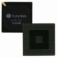
TSI148-133IL IDT, Integrated Device Technology Inc, TSI148-133IL Datasheet - Page 166

TSI148-133IL
Manufacturer Part Number
TSI148-133IL
Description
IC PCI-VME BRIDGE 456PBGA
Manufacturer
IDT, Integrated Device Technology Inc
Series
Tsi148&Trade;r
Datasheets
1.TSI148-133CL.pdf
(391 pages)
2.TSI148-133CL.pdf
(2 pages)
3.TSI148-133CL.pdf
(12 pages)
Specifications of TSI148-133IL
Applications
PCI-to-VME Bridge
Interface
PCI
Voltage - Supply
3.3V
Package / Case
456-PBGA
Mounting Type
Surface Mount
Lead Free Status / RoHS Status
Contains lead / RoHS non-compliant
Other names
800-1905
Available stocks
Company
Part Number
Manufacturer
Quantity
Price
Company:
Part Number:
TSI148-133IL
Manufacturer:
IDT
Quantity:
47
Company:
Part Number:
TSI148-133IL
Manufacturer:
IDT, Integrated Device Technology Inc
Quantity:
10 000
Company:
Part Number:
TSI148-133ILY
Manufacturer:
SUMPLUS
Quantity:
210
Company:
Part Number:
TSI148-133ILY
Manufacturer:
IDT
Quantity:
201
- Current page: 166 of 391
- Download datasheet (2Mb)
8. Signals and Pins > Detailed Signal Descriptions
Table 16: Miscellaneous Signal Descriptions
166
Signal Group
Temperature
Power
Test
TM_IN
TN_OUT
TCK
TMS
TDI
TDO
TRST_
CEO_TEST
VDD2
VDD
VSS
PLL_VDD
PLL_VSS
Signal Name
Active
High
High
High
High
High
Low
I/O
O
I
I
I
I
I
I
I
I
I
I
The TM_IN and TM_OUT signals can be used to measure the die
temperature.
This signal is used to clock state information and test data into and out of
Tsi148 during IEEE 1149.1 test operation.
This signal is used to control the state of the TAP controller during IEEE
1149.1 test operation.
This signal is used to serially shift test data and test instructions into
Tsi148 during IEEE 1149.1 test operation.
This signal is used to serially shift test data and test instructions out of
Tsi148 during IEEE 1149.1 test operation.
This signal provides an asynchronous initialization of the IEEE 1149.1
compliant TAP controller.
This signal must be tied to ground if JTAG is not used in the system.
If JTAG is used in the system, the TRST_ input must be asserted low
at the negation of the PURSTI_ input and then held high during
boundary scan testing.
This signal is used during factory test. It should be pulled down on the
PWB.
The +3.3V pins provide power for the I/O buffers.
The +1.8V pins provide power for the internal core logic.
These pins form the ground connections for all of the input macros,
output macros, and core logic.
The +1.8V pin provides clean power to the internal Analog Phase Locked
Loop.
This input provides clean ground to the internal Analog Phase Locked
Loop.
Tsi148 PCI/X-to-VME Bus Bridge User Manual
Description
80A3020_MA001_13
Related parts for TSI148-133IL
Image
Part Number
Description
Manufacturer
Datasheet
Request
R

Part Number:
Description:
IC PCI-VME BRIDGE 456PBGA
Manufacturer:
IDT, Integrated Device Technology Inc
Datasheet:

Part Number:
Description:
TRANSLATION DEVICE DPI 80-PQFP
Manufacturer:
IDT, Integrated Device Technology Inc
Datasheet:

Part Number:
Description:
IDT PART
Manufacturer:
IDT, Integrated Device Technology Inc
Datasheet:

Part Number:
Description:
IC LIU T1/E1/J1 OCTAL 256PBGA
Manufacturer:
IDT, Integrated Device Technology Inc
Datasheet:

Part Number:
Description:
IC FREQ TIMING GENERATOR 28TSSOP
Manufacturer:
IDT, Integrated Device Technology Inc
Datasheet:

Part Number:
Description:
IC CLK DVR PLL 1:10 40VFQFPN
Manufacturer:
IDT, Integrated Device Technology Inc
Datasheet:

Part Number:
Description:
IC CLK FANOUT BUFFER 1:18 32LQFP
Manufacturer:
IDT, Integrated Device Technology Inc
Datasheet:

Part Number:
Description:
IC CLK FANOUT BUFFER 1:18 32LQFP
Manufacturer:
IDT, Integrated Device Technology Inc
Datasheet:

Part Number:
Description:
IC CK505 VREG/RES 56TSSOP
Manufacturer:
IDT, Integrated Device Technology Inc
Datasheet:

Part Number:
Description:
IC SDRAM CLK DVR 1:10 48-TSSOP
Manufacturer:
IDT, Integrated Device Technology Inc
Datasheet:

Part Number:
Description:
IC CLK DVR PLL 1:10 48TSSOP
Manufacturer:
IDT, Integrated Device Technology Inc
Datasheet:

Part Number:
Description:
IC FLEXPC CLK PROGR P4 56-TSSOP
Manufacturer:
IDT, Integrated Device Technology Inc
Datasheet:

Part Number:
Description:
IC FLEXPC CLK PROGR P4 56-TSSOP
Manufacturer:
IDT, Integrated Device Technology Inc
Datasheet:

Part Number:
Description:
IC FLEXPC CLK PROGR P4 56-SSOP
Manufacturer:
IDT, Integrated Device Technology Inc
Datasheet:

Part Number:
Description:
IC PLL CLK DRIVER 2.5V 28-TSSOP
Manufacturer:
IDT, Integrated Device Technology Inc
Datasheet:


