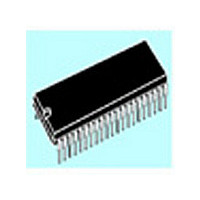
ST72T774J9B1 STMicroelectronics, ST72T774J9B1 Datasheet - Page 107

ST72T774J9B1
Manufacturer Part Number
ST72T774J9B1
Description
Manufacturer
STMicroelectronics
Datasheet
1.ST72T774J9B1.pdf
(144 pages)
Specifications of ST72T774J9B1
Cpu Family
ST7
Device Core Size
8b
Frequency (max)
24MHz
Interface Type
I2C/USB
Program Memory Type
EPROM
Program Memory Size
60KB
Total Internal Ram Size
1KB
# I/os (max)
31
Number Of Timers - General Purpose
1
Operating Supply Voltage (typ)
5V
Operating Supply Voltage (max)
5.5V
Operating Supply Voltage (min)
4V
On-chip Adc
1-chx8-bit
On-chip Dac
1-chx8-bit
Instruction Set Architecture
CISC
Operating Temp Range
0C to 70C
Operating Temperature Classification
Commercial
Mounting
Through Hole
Pin Count
42
Package Type
SPDIP
Lead Free Status / Rohs Status
Specific Sites Compliant
Available stocks
Company
Part Number
Manufacturer
Quantity
Price
Part Number:
ST72T774J9B1
Manufacturer:
ST
Quantity:
20 000
DDC INTERFACE (Cont’d)
4.8.5.2 DDC/CI - Factory Alignment Interface
4.8.5.2.1 Functional Description
Refer to the CR, SR1 and SR2 registers in
4.8.6. for the bit definitions.
The DDC/CI interface works as an I/O interface
between the microcontroller and the DDC2Bi,
EDDC or Factory alignment protocols. It receives
and transmits data in Slave I
interrupt or polled handshaking.
The interface is connected to the I
pin (SDAD) and a clock pin (SCLD) configured as
open drain.
The DDC/CI interface has five internal register
locations.
Two of them are used for initialization of the
interface:
– Own Address Register OAR
– Control register CR
The following four registers are used during data
transmission/reception:
– Data Register DR
– Control Register CR
– Status Register 1 SR1
– Status Register 2 SR2
The interface decodes an I
stored by software in the OAR register and/or the
EDDC address (60h/61h) as its default hardware
address.
After a reset, the interface is disabled.
2
C or DDC2Bi address
2
C mode using an
2
C bus by a data
Section
4.8.5.2.2 I
In I
following modes:
– Slave transmitter/receiver
Both start and stop conditions are generated by
the master. The I2C clock (SCL) is always
received by the interface from a master, but the
interface is able to stretch the clock line.
The interface is capable of recognizing both its
own programmable address (7-bit) and its default
hardware address (Enhanced DDC address: 60h/
61h). The Enhanced DDC address detection may
be enabled or disabled by software. It never
recognizes the Start byte (01h) whatever its own
address is.
As soon as a start condition is detected, the
address is received from the SDA line and sent to
the shift register; then it is compared with the
programmable address of the interface or the
Enhanced DDC address (if selected by software).
Address not matched: the interface ignores it
and waits for another Start condition.
Address matched: the following events occur in
sequence:
– Acknowledge pulse is generated if the ACK bit is
– EVF and ADSL bits are set.
– An interrupt is generated if the ITE bit is set.
Then the interface waits for a read of the SR1
register, holding the SCL line low (see
Transfer sequencing EV1).
Next, the DR register must be read to determine
from the least significant bit if the slave must enter
Receiver or Transmitter mode.
set.
General description
Slave Mode
2
C mode, the interface can operate in the
2
C Modes
ST72774/ST727754/ST72734
Figure 67
107/144


