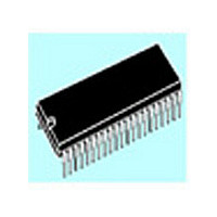
ST72T774J9B1 STMicroelectronics, ST72T774J9B1 Datasheet - Page 50

ST72T774J9B1
Manufacturer Part Number
ST72T774J9B1
Description
Manufacturer
STMicroelectronics
Datasheet
1.ST72T774J9B1.pdf
(144 pages)
Specifications of ST72T774J9B1
Cpu Family
ST7
Device Core Size
8b
Frequency (max)
24MHz
Interface Type
I2C/USB
Program Memory Type
EPROM
Program Memory Size
60KB
Total Internal Ram Size
1KB
# I/os (max)
31
Number Of Timers - General Purpose
1
Operating Supply Voltage (typ)
5V
Operating Supply Voltage (max)
5.5V
Operating Supply Voltage (min)
4V
On-chip Adc
1-chx8-bit
On-chip Dac
1-chx8-bit
Instruction Set Architecture
CISC
Operating Temp Range
0C to 70C
Operating Temperature Classification
Commercial
Mounting
Through Hole
Pin Count
42
Package Type
SPDIP
Lead Free Status / Rohs Status
Specific Sites Compliant
Available stocks
Company
Part Number
Manufacturer
Quantity
Price
Part Number:
ST72T774J9B1
Manufacturer:
ST
Quantity:
20 000
ST72774/ST727754/ST72734
16-BIT TIMER (Cont’d)
4.3.3.7 Pulse Width Modulation Mode
Pulse Width Modulation mode enables the
generation of a signal with a frequency and pulse
length determined by the value of the OC1R and
OC2R registers.
The pulse width modulation mode uses the
complete Output Compare 1 function plus the
OC2R register.
Procedure
To use pulse width modulation mode select the
following in the CR1 register:
– Using the OLVL1 bit, select the level to be ap-
– Using the OLVL2 bit, select the level to be ap-
And select the following in the CR2 register:
– Set OC1E bit: the OCMP1 pin is then dedicated
– Set the PWM bit.
– Select the timer clock (CC1-CC0) (see
Load
corresponding to the period of the signal.
Load
corresponding to the length of the pulse if
(OLVL1=0 and OLVL2=1).
If OLVL1=1 and OLVL2=0 the length of the pulse is
the difference between the OC2R and OC1R
registers.
Figure 36. Pulse Width Modulation Mode Timing
50/144
plied to the OCMP1 pin after a successful com-
parison with OC1R register.
plied to the OCMP1 pin after a successful com-
parison with OC2R register.
to the output compare 1 function.
Clock Control
the
the
COUNTER
OCMP1
OC2R
OC1R
Note: OC1R=2ED0h, OC2R=34E2, OLVL1=0, OLVL2= 1
Bits).
compare2
register
register
34E2
FFFC FFFD FFFE
with
with
the
the
Table 15
OLVL2
value
value
The OC
timing application can be calculated using the
following formula:
Where:
The Output Compare 2 event causes the counter
to be initialized to FFFCh (See
Note: After a write instruction to the OC i HR register, the
The OCF1 and OCF2 bits cannot be set by
hardware in PWM mode therefore the Output
Compare interrupt is inhibited. The Input Capture
interrupts are available.
When the Pulse Width Modulation (PWM) and
One Pulse Mode (OPM) bits are both set, the
PWM mode is the only active one.
– t = Desired output compare period (seconds)
– f
– CC1-CC0 = Timer clock prescaler
compare1
neous register)
2ED0 2ED1 2ED2
CPU
output compare function is inhibited until the OC i LR
register is also written.
i
R register value required for a specific
Counter
= OC1R
OC i R Value =
= Internal clock frequency (see Miscella-
Counter
= OC2R
When
When
OLVL1
Pulse Width Modulation cycle
compare2
(CC1.CC0)
OCMP1 = OLVL2
t
OCMP1 = OLVL1
34E2
Counter is reset
*
f
CPU
to FFFCh
Figure
OLVL2
FFFC
- 5
36).


