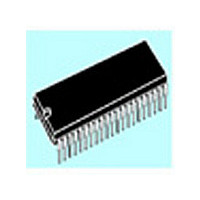
ST72T774J9B1 STMicroelectronics, ST72T774J9B1 Datasheet - Page 110

ST72T774J9B1
Manufacturer Part Number
ST72T774J9B1
Description
Manufacturer
STMicroelectronics
Datasheet
1.ST72T774J9B1.pdf
(144 pages)
Specifications of ST72T774J9B1
Cpu Family
ST7
Device Core Size
8b
Frequency (max)
24MHz
Interface Type
I2C/USB
Program Memory Type
EPROM
Program Memory Size
60KB
Total Internal Ram Size
1KB
# I/os (max)
31
Number Of Timers - General Purpose
1
Operating Supply Voltage (typ)
5V
Operating Supply Voltage (max)
5.5V
Operating Supply Voltage (min)
4V
On-chip Adc
1-chx8-bit
On-chip Dac
1-chx8-bit
Instruction Set Architecture
CISC
Operating Temp Range
0C to 70C
Operating Temperature Classification
Commercial
Mounting
Through Hole
Pin Count
42
Package Type
SPDIP
Lead Free Status / Rohs Status
Specific Sites Compliant
Available stocks
Company
Part Number
Manufacturer
Quantity
Price
Part Number:
ST72T774J9B1
Manufacturer:
ST
Quantity:
20 000
ST72774/ST727754/ST72734
DDC INTERFACE (Cont’d)
4.8.6 Register Description
DDC CONTROL REGISTER (CR)
Read / Write
Reset Value: 0000 0000 (00h)
Bit 7:6 = Reserved. Forced to 0 by hardware.
Bit 5 = PE Peripheral enable.
This bit is set and cleared by software.
0: Peripheral disabled
1: Slave capability
Notes:
– When PE=0, all the bits of the CR register and
– When PE=1, the corresponding I/O pins are se-
– To enable the I
Bit 4 = EDDCEN Enhanced DDC address
detection enabled.
This bit is set and cleared by software. It is also
cleared by hardware when the interface is disabled
(PE=0). The 60h/61h Enhanced DDC address is
acknowledged.
0: Enhanced DDC address detection disabled
1: Enhanced DDC address detection enabled
110/144
the SR register are reset. All outputs are re-
leased while PE=0
lected by hardware as alternate functions.
TWICE with PE=1 as the first write only activates
the interface (only PE is set).
7
0
0
PE
2
C interface, write the CR register
EDDC
EN
0
ACK
STOP
ITE
0
Bit 3 = Reserved. Forced to 0 by hardware.
Bit 2 = ACK Acknowledge enable.
This bit is set and cleared by software. It is also
cleared by hardware when the interface is disabled
(PE=0).
0: No acknowledge returned
1: Acknowledge returned after an address byte or
Bit 1 = STOP Release I2C bus .
This bit is set and cleared by software or when the
interface is disabled (PE=0).
– Slave Mode:
Bit 0 = ITE Interrupt enable.
This bit is set and cleared by software and cleared
by hardware when the interface is disabled
(PE=0).
0: Interrupts disabled
1: Interrupts enabled
Refer to
events and the interrupt.
SCL is held low when the BTF or ADSL is detect-
ed.
0: Nothing
1: Release the SCL and SDA lines after the cur-
rent byte transfer (BTF=1). The STOP bit has to
be cleared by software.
a data byte is received
Figure 68
for the relationship between the


