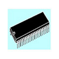
ST72T774J9B1 STMicroelectronics, ST72T774J9B1 Datasheet - Page 31

ST72T774J9B1
Manufacturer Part Number
ST72T774J9B1
Description
Manufacturer
STMicroelectronics
Datasheet
1.ST72T774J9B1.pdf
(144 pages)
Specifications of ST72T774J9B1
Cpu Family
ST7
Device Core Size
8b
Frequency (max)
24MHz
Interface Type
I2C/USB
Program Memory Type
EPROM
Program Memory Size
60KB
Total Internal Ram Size
1KB
# I/os (max)
31
Number Of Timers - General Purpose
1
Operating Supply Voltage (typ)
5V
Operating Supply Voltage (max)
5.5V
Operating Supply Voltage (min)
4V
On-chip Adc
1-chx8-bit
On-chip Dac
1-chx8-bit
Instruction Set Architecture
CISC
Operating Temp Range
0C to 70C
Operating Temperature Classification
Commercial
Mounting
Through Hole
Pin Count
42
Package Type
SPDIP
Lead Free Status / Rohs Status
Specific Sites Compliant
Available stocks
Company
Part Number
Manufacturer
Quantity
Price
Part Number:
ST72T774J9B1
Manufacturer:
ST
Quantity:
20 000
I/O PORTS (Cont’d)
4.1.4 Port B
The alternate functions are the I/O pins of the on-
chip DDC SCLD & SCDAD for PB0:1, the I/O pins
of the on-chip I2C SCLI & SCDAI for PB2:3, and 4
bits of port B bit can be used as the Analog source
to the Analog to Digital Converter.
Only one I/O line must be configured as an analog
input at any time. The user must avoid any
situation in which more than one I/O pin is selected
as an analog input simultaneously to avoid device
malfunction.
When the analog function is selected for an I/O pin,
the pull-up of the respective pin of Port B is
disconnected and the digital input is off.
Table 9. Port B Description
PB0
PB1
PB2
PB3
PB4
PB5
PB6
PB7
*Reset state
PORT B
Without pull-up
Without pull-up
Without pull-up
Without pull-up
With pull-up
With pull-up
With pull-up
With pull-up
Input*
I/O
Open-drain
Open-drain
Open-drain
Open-drain
Push-pull
Push-pull
Push-pull
Push-pull
Output
SCLD (input with CMOS schmitt trigger or
open drain output)
SDAD (input with CMOS schmitt trigger or
open drain output)
SCLI (input with CMOS schmitt trigger or
open drain output)
SDAI (input with CMOS schmitt trigger or
open drain output)
Analog input (ADC) (without pull-up)
Analog input (ADC) (without pull-up)
Analog input (ADC) (without pull-up)
10-bit output 1 (PWM)
Analog input (ADC) (without pull-up)
10-bit output 2 (PWM)
All unused I/O lines should be tied to an
appropriate logic level (either V
Since the ADC is on the same chip as the
microprocessor, the user should not switch heavily
loaded signals during conversion, if high precision
is required. Such switching will affect the supply
voltages used as analog references. the accuracy
of the conversion depends on the quality of the
power supplies (V
special care to ensure that a well regulated
reference voltage is present on the V
pins (power supply variations must be less than
5V/ms). This implies, in particular, that a suitable
decoupling capacitor is used at the V
Signal
Alternate Function
ST72774/ST727754/ST72734
DD
and V
SS
DDC enable
DDC enable
I2C enable
I2C enable
CH[2:0]=000 (ADCCSR)
CH[2:0]=001 (ADCCSR)
CH[2:0]=010 (ADCCSR)
OE0=1 (PWMOE)
CH[2:0]=011 (ADCCSR)
OE1=1 (PWMOE)
). The user must take
DD
Condition
or V
DD
DD
SS
pin.
)
and V
31/144
SS


