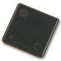
H5PS1G83EFR-S6C HYNIX SEMICONDUCTOR, H5PS1G83EFR-S6C Datasheet - Page 28

H5PS1G83EFR-S6C
Manufacturer Part Number
H5PS1G83EFR-S6C
Description
58T1895
Manufacturer
HYNIX SEMICONDUCTOR
Datasheet
1.H5PS1G83EFR-S6C.pdf
(44 pages)
Specifications of H5PS1G83EFR-S6C
Memory Type
SDRAM
Memory Configuration
128M X 8
Access Time
15ns
Memory Case Style
FBGA
No. Of Pins
60
Operating Temperature Range
0°C To +85°C
Memory Size
1 Gbit
Rohs Compliant
Yes
Available stocks
Company
Part Number
Manufacturer
Quantity
Price
Company:
Part Number:
H5PS1G83EFR-S6C
Manufacturer:
HYNIX
Quantity:
4 000
Part Number:
H5PS1G83EFR-S6C
Manufacturer:
HYNIX/海力士
Quantity:
20 000
Company:
Part Number:
H5PS1G83EFR-S6C-C
Manufacturer:
HYNIX
Quantity:
9 500
Company:
Part Number:
H5PS1G83EFR-S6C-C
Manufacturer:
HYNIX
Quantity:
135
Company:
Part Number:
H5PS1G83EFR-S6C-C-6Z
Manufacturer:
HYNIX
Quantity:
5 361
Rev. 0.4 / Nov 2008
Specific Notes for dedicated AC parameters
1. User can choose which active power down exit timing to use via MRS(bit 12). tXARD is expected to be
used for fast active power down exit timing. tXARDS is expected to be used for slow active power down exit
timing where a lower power value is defined by each vendor data sheet.
2. AL = Additive Latency
3. This is a minimum requirement. Minimum read to precharge timing is AL + BL/2 providing the tRTP and
tRAS(min) have been satisfied.
4. A minimum of two clocks (2 * tCK or 2 * nCK) is required irrespective of operating frequency
5. Timings are specified with command/address input slew rate of 1.0 V/ns. See System Derating for other
slew rate values.
6. Timings are guaranteed with DQs, DM, and DQS’s(DQS/RDQS in singled ended mode) input slew rate of
1.0 V/ns. See System Derating for other slew rate values.
7. Timings are specified with CK/CK differential slew rate of 2.0 V/ns. Timings are guaranteed for DQS signals
with a differential slew rate of 2.0 V/ns in differential strobe mode and a slew rate of 1V/ns in single ended
mode. See System Derating for other slew rate values.
8. tDS and tDH derating
1) For all input signals the total tDS(setup time) and tDH(hold time) required is calculated by adding the datasheet value to the derating
Slew
Slew
V/ns
V/ns
rate
rate
DQ
DQ
2.0
1.5
1.0
0.9
0.8
0.7
0.6
0.5
0.4
2.0
1.5
1.0
0.9
0.8
0.7
0.6
0.5
0.4
tDS, tDH Derating Values for DDR2-400, DDR2-533(ALL units in 'ps', Note 1 applies to entire Table)
tDS, tDH Derating Values for DDR2-667, DDR2-800(ALL units in 'ps', Note 1 applies to entire Table)
125
100
tDS
tDS
83
67
△
4.0 V/ns
△
0
4.0 V/ns
0
-
-
-
-
-
-
-
-
-
-
-
-
tDH
tDH
45
21
45
21
△
△
0
0
-
-
-
-
-
-
-
-
-
-
-
-
125
100
tDS
tDS
-11
83
67
△
△
-5
3.0 V/ns
0
3.0 V/ns
0
-
-
-
-
-
-
-
-
-
-
tDH
tDH
-14
-14
45
21
△
45
21
△
0
0
-
-
-
-
-
-
-
-
-
-
+125 +45
+83
tDS
100
tDS
-11
-25
-13
△
67
△
-5
2.0 V/ns
2.0 V/ns
0
0
-
-
-
-
-
-
-
-
+21
tDH
tDH
-14
-31
-14
-31
△
45
21
△
0
0
-
-
-
-
-
-
-
-
tDS
-13
-31
tDS
-10
95
12
△
79
12
1.8 V/ns
△
-1
1.8 V/ns
1
7
DQS, DQS Differential Slew Rate
-
-
-
-
DQS, DQS Differential Slew Rate
-
-
-
-
tDH
-19
-42
tDH
-19
-42
33
12
33
△
-2
12
△
-2
-
-
-
-
-
-
-
-
tDS
-42
-43
tDS
-10
24
13
24
19
11
△
-1
1.6 V/ns
△
1.6 V/ns
2
-
-
-
-
-
-
-
-
tDH
-19
-59
tDH
-30
-59
24
10
24
10
△
-7
△
-7
-
-
-
-
-
-
-
-
tDS
-31
-74
tDS
-24
11
25
31
23
14
△
-7
1.4 V/ns
△
1.4 V/ns
2
-
-
-
-
-
-
-
-
tDH
-47
-89
tDH
-18
-47
-89
22
22
△
-8
△
5
5
-
-
-
-
-
-
-
-
-127 -140 -115 -128 -103 -116
tDS
tDS
-19
-62
-12
-52
23
35
26
14
△
△
1.2 V/ns
1.2 V/ns
5
-
-
-
-
-
-
-
-
-140
tDH
tDH
-35
-77
-35
-77
17
△
-6
17
△
-6
-
-
-
-
-
-
-
-
H5PS1G43EFR
H5PS1G83EFR
H5PS1G63EFR
tDS
tDS
-50
-40
17
△
-7
38
26
△
1.0 V/ns
1.0 V/ns
0
-
-
-
-
-
-
-
-
-
-
-128
tDH
-23
-65
tDH
-23
-65
△
△
6
6
-
-
-
-
-
-
-
-
-
-
tDS
-38
tDS
-28
△
38
12
0.8 V/ns
△
0.8 V/ns
5
-
-
-
-
-
-
-
-
-
-
-
-
-116
tDH
-11
-53
tDH
-11
-53
△
28
△
-
-
-
-
-
-
-
-
-
-
-
-


