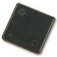
H5PS1G83EFR-S6C HYNIX SEMICONDUCTOR, H5PS1G83EFR-S6C Datasheet - Page 4

H5PS1G83EFR-S6C
Manufacturer Part Number
H5PS1G83EFR-S6C
Description
58T1895
Manufacturer
HYNIX SEMICONDUCTOR
Datasheet
1.H5PS1G83EFR-S6C.pdf
(44 pages)
Specifications of H5PS1G83EFR-S6C
Memory Type
SDRAM
Memory Configuration
128M X 8
Access Time
15ns
Memory Case Style
FBGA
No. Of Pins
60
Operating Temperature Range
0°C To +85°C
Memory Size
1 Gbit
Rohs Compliant
Yes
Available stocks
Company
Part Number
Manufacturer
Quantity
Price
Company:
Part Number:
H5PS1G83EFR-S6C
Manufacturer:
HYNIX
Quantity:
4 000
Part Number:
H5PS1G83EFR-S6C
Manufacturer:
HYNIX/海力士
Quantity:
20 000
Company:
Part Number:
H5PS1G83EFR-S6C-C
Manufacturer:
HYNIX
Quantity:
9 500
Company:
Part Number:
H5PS1G83EFR-S6C-C
Manufacturer:
HYNIX
Quantity:
135
Company:
Part Number:
H5PS1G83EFR-S6C-C-6Z
Manufacturer:
HYNIX
Quantity:
5 361
Note:
-XX* is the speed bin, refer to the Operating Frequency table for complete part number.
Hynix lead & halogen-free products are compliant to RoHS.
Rev. 0.4 / Nov 2008
1. Description
Ordering Information
H5PS1G43EFR-XX*
H5PS1G83EFR-XX*
H5PS1G63EFR-XX*
1.1 Device Features & Ordering Information
1.1.1 Key Features
• VDD = 1.8 +/- 0.1V
• VDDQ = 1.8 +/- 0.1V
• All inputs and outputs are compatible with SSTL_18 interface
• 8 banks
• Fully differential clock inputs (CK, /CK) operation
• Double data rate interface
• Source synchronous-data transaction aligned to bidirectional data strobe (DQS, DQS)
• Differential Data Strobe (DQS, DQS)
• Data outputs on DQS, DQS edges when read (edged DQ)
• Data inputs on DQS centers when write (centered DQ)
• On chip DLL align DQ, DQS and DQS transition with CK transition
• DM mask write data-in at the both rising and falling edges of the data strobe
• All addresses and control inputs except data, data strobes and data masks latched on the rising
• Programmable CAS latency 3, 4, 5 and 6 supported
• Programmable additive latency 0, 1, 2, 3, 4 and 5 supported
• Programmable burst length 4/8 with both nibble sequential and interleave mode
• Internal eight bank operations with single pulsed RAS
• Auto refresh and self refresh supported
• tRAS lockout supported
• 8K refresh cycles /64ms
• JEDEC standard 60ball FBGA(x4/x8), 84ball FBGA(x16)
• Full strength driver option controlled by EMR
• On Die Termination supported
• Off Chip Driver Impedance Adjustment supported
• Read Data Strobe supported (x8 only)
• Self-Refresh High Temperature Entry
edges of the clock
Part No.
Configuration Package
256Mx4
128Mx8
64Mx16
60 Ball
84 Ball
Operating Frequency
Grade
E3
C4
Y5
S6
S5
tCK(ns)
3.75
2.5
2.5
5
3
CL
3
4
5
6
5
tRCD
3
4
5
6
5
H5PS1G43EFR
H5PS1G83EFR
H5PS1G63EFR
tRP
3
4
5
6
5
Unit
Clk
Clk
Clk
Clk
Clk
4


