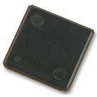
H5PS1G83EFR-S6C HYNIX SEMICONDUCTOR, H5PS1G83EFR-S6C Datasheet - Page 29

H5PS1G83EFR-S6C
Manufacturer Part Number
H5PS1G83EFR-S6C
Description
58T1895
Manufacturer
HYNIX SEMICONDUCTOR
Datasheet
1.H5PS1G83EFR-S6C.pdf
(44 pages)
Specifications of H5PS1G83EFR-S6C
Memory Type
SDRAM
Memory Configuration
128M X 8
Access Time
15ns
Memory Case Style
FBGA
No. Of Pins
60
Operating Temperature Range
0°C To +85°C
Memory Size
1 Gbit
Rohs Compliant
Yes
Available stocks
Company
Part Number
Manufacturer
Quantity
Price
Company:
Part Number:
H5PS1G83EFR-S6C
Manufacturer:
HYNIX
Quantity:
4 000
Part Number:
H5PS1G83EFR-S6C
Manufacturer:
HYNIX/海力士
Quantity:
20 000
Company:
Part Number:
H5PS1G83EFR-S6C-C
Manufacturer:
HYNIX
Quantity:
9 500
Company:
Part Number:
H5PS1G83EFR-S6C-C
Manufacturer:
HYNIX
Quantity:
135
Company:
Part Number:
H5PS1G83EFR-S6C-C-6Z
Manufacturer:
HYNIX
Quantity:
5 361
Rev. 0.4 / Nov 2008
value listed in Table x.
Setup(tDS) nominal slew rate for a rising signal is defined as the slew rate between the last crossing of VREF(dc) and the first crossing
of Vih(ac)min. Setup(tDS) nominal slew rate for a falling signal is defined as the slew rate between the last crossing of VREF(dc) and the
first crossing of Vil(ac)max. If the actual signal is always earlier than the nominal slew rate line between shaded ‘ VREF(dc) to ac region’,
use nominal slew rate for derating value(see Fig a.) If the actual signal is later than the nominal slew rate line anywhere between shaded
‘VREF(dc) to ac region’, the slew rate of a tangent line to the actual signal from the ac level to dc level is used for derating value(see Fig b.)
Hold(tDH) nominal slew rate for a rising signal is defined as the slew rate between the last crossing of Vil(dc) max and the first crossing
of VREF(dc). Hold (tDH) nominal slew rate for a falling signal is defined as the slew rate between the last crossing of Vih(dc) min and the
first crossing of VREF(dc). If the actual signal is always later than the nominal slew rate line anywhere between shaded ‘dc to VREF(dc)
region’, the slew rate of a tangent line to the actual signal from the dc level to VREF(dc) level is used for derating value(see Fig c.) If the
actual signal is earlier than the nominal slew rate line anywhere between shaded ‘dc to VREF(dc) region’, the slew rate of a tangent line
to the actual signal from the dc level to VREF(dc) level is used for derating value(see Fig d.)
Although for slow slew rates the total setup time might be negative(i.e. a valid input signal will not have reached VIH/IL(ac) at the time
of the rising clock transition) a valid input signal is still required to complete the transition and reach VIH/IL(ac).
For slew rate in between the values listed in table x, the derating valued may obtained by linear interpolation.
These values are typically not subject to production test. They are verified by design and characterization.
Slew
V/ns
rate
DQ
2.0
1.5
1.0
0.9
0.8
0.7
0.6
0.5
0.4
tDS, tDH Derating Values for DDR2-400, DDR2-533(ALL units in 'ps', Note 1 applies to entire Table)
188
146
tDS
63
△
4.0 V/ns
-
-
-
-
-
-
188
167
125
tDH
△
-
-
-
-
-
-
167
125
tDS
42
31
△
3.0 V/ns
-
-
-
-
-
146
125
tDH
83
69
△
-
-
-
-
-
125
tDS
-11
-25
83
△
2.0 V/ns
0
-
-
-
-
tDH
-14
-31
63
42
△
0
-
-
-
-
tDS
DQS, DQS Single-ended Slew Rate
-13
-27
-45
81
△
-2
1.8 V/ns
-
-
-
-
tDH
-13
-30
-53
43
△
1
-
-
-
-
tDS
-18
-32
-50
-74
△
-7
1.6 V/ns
-
-
-
-
tDH
-13
-27
-44
-67
-96
△
-
-
-
-
-128 -156 -145 -180 -175 -223 -226 -288
tDS
-29
-43
-61
-85
△
1.4 V/ns
-
-
-
-
-114 -102 -138 -132 -181 -183 -248
tDH
-45
-62
-85
△
-
-
-
-
-210 -243 -240 -286 -291 -351
tDS
-60
-78
△
1.2 V/ns
-
-
-
-
-109 -108 -152
tDH
-86
△
-
-
-
-
H5PS1G43EFR
H5PS1G83EFR
H5PS1G63EFR
tDS
△
1.0 V/ns
-
-
-
-
-
tDH
△
-
-
-
-
-
tDS
△
0.8 V/ns
-
-
-
-
-
-
29
tDH
△
-
-
-
-
-
-


