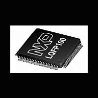
XA-H3 NXP Semiconductors, XA-H3 Datasheet - Page 11

XA-H3
Manufacturer Part Number
XA-H3
Description
The powerful 16-bit XA CPU core and rich feature set make the XA-H3 and XA-H4 devices ideal for high-performance real-time applications such as industrial control and networking
Manufacturer
NXP Semiconductors
Datasheet
1.XA-H3.pdf
(36 pages)
*
# SFRs marked with a pound sign (#) are additional SFR registers specific to the XA-H3 and XA-H4.
1. The XA-H3 implements an 8-bit SFR bus, as stated in Chapter 8 of the IC25 Data Handbook XA User Guide . All SFR accesses must be
2. SFR is loaded from the reset vector.
3. F1, F0, and P reset to “0”. All other bits are loaded from the reset vector.
4. Unimplemented bits in SFRs are “X” (unknown) at all times. “1”s should not be written to these bits since they may be used for other
5. Port configurations default to quasi-bidirectional when the XA begins execution after reset. Thus all PnCFGA registers will contain FFh and
6. The WDCON reset value is E6 for a Watchdog reset; E4 for all other reset causes.
7. The RSTSRC register reflects the cause of the last XA reset. One bit will be set to “1”, the others will be “0”. RSTSRC[7] enables the ResetOut
8. The XA guards writes to certain bits (typically interrupt flags) that may be written by a peripheral function. This prevents loss of an interrupt or
Philips Semiconductors
NOTES:
1999 Sep 24
TSTAT*
WDCON*
WDL
WFEED1
WFEED2
CMOS 16-bit highly integrated microcontroller
Name
SFRs marked with an asterisk (*) are bit addressable.
8-bit operations. Attempts to write 16 bits to an SFR will actually write only the lower 8 bits. 16-bit SFR reads will return undefined data in the
upper byte.
purposes in future XA derivatives. The reset value shown for these bits is “0”.
PnCFGB register will contain 00h. See warning in XA-H3 User Manual about P3.2_Timer0_ResetOut pin during first 258 clocks after power
up. Basically, during this period, this pin may output a strongly-driven low pulse. If the pulse does occur, it will terminate in a transition to high
at a time no later than the 259th system clock after valid V
function; “1” = Enabled, “0” = Disabled. See XA-H3 User Manual for details; RSTSRC[7] differs in function from most other XA derivatives.
other status if a bit was written directly by a peripheral action between the read and write of an instruction that performs a read-modify-write
operation. XA-H3 SFR bits that are guarded in this manner are: TF1, TF0, IE1, and IE0 (in TCON), and WDTOF (in WDCON).
Timer 0/1 Extended Status
Watchdog Control
Watchdog Timer Reload
Watchdog Feed 1
Watchdog Feed 2
Description
411h
41Fh
45Fh
45Dh
45Eh
Address
SFR
PRE2
MSB
28F
2FF
–
CC
PRE1
power up.
28E
2FE
–
11
PRE0
28D
2FD
–
Bit Functions and Addresses
28C
2FC
–
–
28B
2FB
–
–
WDRUN
T1OE
28A
2FA
WDTOF
2F9
289
–
Preliminary specification
T0OE
LSB
288
2F8
XA-H3
–
Reset
Value
00h
00h
6
x
x


