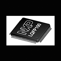
XA-H3 NXP Semiconductors, XA-H3 Datasheet - Page 7

XA-H3
Manufacturer Part Number
XA-H3
Description
The powerful 16-bit XA CPU core and rich feature set make the XA-H3 and XA-H4 devices ideal for high-performance real-time applications such as industrial control and networking
Manufacturer
NXP Semiconductors
Datasheet
1.XA-H3.pdf
(36 pages)
Philips Semiconductors
PIN DESCRIPTIONS
1999 Sep 24
Mnemonic
See Pins 56, 57 for 2 additional Chip Selects
D15 – D0
XTALOut
A19 – A0
CMOS 16-bit highly integrated microcontroller
ResetIn
XTALIn
Size16
ClkOut
WAIT/
TxD0
BHE
P0.0
P0.1
P0.2
P0.3
P0.4
P0.5
P0.6
P0.7
CS0
CS1
CS2
CS3
BLE
V
V
WE
OE
SS
DD
1, 19, 28,
2, 20, 29,
Pin No.
24 – 21,
42 – 30,
27 – 25
44, 59,
43, 62,
18 – 3
76, 88
77, 89
Lqfp
100
55
52
60
61
49
48
47
46
50
51
54
53
45
90
91
92
93
94
95
99
96
Type
I/O
I/O
I/O
I/O
I/O
I/O
I/O
I/O
I/O
O
O
O
O
O
O
O
O
O
O
O
I
I
I
I
I
I
Ground: 0 V reference.
Power Supply: This is the power supply voltage for normal, idle, and power down operation.
Reset: A low on this pin resets the microcontroller, causing I/O ports and peripherals to take on
their default states, and the processor to begin execution at the address contained in the reset
vector.
Wait/Size16: During Reset, this input determines bus size for boot device (“1” = 16-bit boot device;
“0” = 8-bit.) During normal operation this is the Wait input (“1” = Wait; “0” = Proceed.)
Crystal 1: Input to the inverting amplifier used in the oscillator circuit and input to the internal clock
generator circuits.
Crystal 2: Output from the oscillator amplifier.
Chip Select 0: This output provides the active low chip select to the boot device (usually ROM or
Flash.) From reset, it is enabled and mapped to an address range based at 000000h. It can be
remapped by software to a higher base in the address map (see the “Memory Interface” chapter in
the XA-H3 User Manual .)
Chip Select 1*: Chip Selects 1 through 5 come out of reset disabled. They function as normal chip
selects on the H3. CS1 can be “swapped” with CS0 (see the SWAP operation in the “Memory
Controller” chapter of the XA-H3 User Manual .) CS1 is usually mapped to be based at 000000h
after the swap, but is capable of being based anywhere in the 16 MB address space.
Chip Select 2 *: Active low Chip Selects CS1 through CS5 come out of reset disabled. They can
be programmed to function as normal chip selects. CS2 through CS5 are not used with the
“SWAP” operation (only /CS0 and CS1 can be swapped; see “Memory Controller” chapter in the
XA-H3 User Manual .) They are mappable to any region of the 16 MB address space.
Chip Select 3 *: See Chip Select 2 for description.
Write Enable: Goes active low during all bus write cycles only.
Output Enable: Goes active low during all bus read cycles only.
Byte Low Enable: Goes active low during all bus cycles that access data bus lines D7 – D0, read
or write.
Byte High Enable: Goes active low during all bus cycles that access data bus lines D15 – D8,
read or write. Never goes active on an 8-bit bus; always goes active on Reads or Fetches on a
16-bit bus, even if the processor does not need these bits. In other words, all Reads (byte or word)
on a 16-bit bus, assert BHE.
Clock Output: This pin outputs a buffered version of the internal CPU clock. The clock output may
be used in conjunction with the external bus to synchronize WAIT state generators, etc. The clock
output may be disabled by software. WARNING: The capacitive loading on this output must not
exceed 40 pf.
Address[19:0]: These address lines output A19 – A0 during all external bus cycles.
Data[15:0]: Bi-directional data bus, D15 – D0; for those bus cycles that are programmed to occur
on an “8-bit bus”, D15 – D8 are unused.
P0.0_BRG0*: Port 0 Bit 0, or UART0 BRG output, or UART0 TxClk output
P0.1_RTS0: Port 0 Bit 1 , or UART0 RTS (Request To Send) output.
P0.2_CTS0: Port 0 Bit 2, or UART0 CTS (Clear To Send) input.
P0.3_CD0: Port 0 Bit 3, or UART0 Carrier Detect input.
P0.4_TRClk0: Port 0 Bit 4, or UART0 TR clock input.
P0.5_RTClk0: Port 0 Bit 5, or UART0 RT clock input.
P0.6: Port 0 Bit 6
P0.7: Port 0 Bit 7
TxD0: Transmit data for UART0.
7
Name and Function
Preliminary specification
XA-H3
Note
See
1, 2
1, 2
1
1
1
1
1
1


