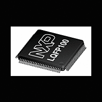
XA-H3 NXP Semiconductors, XA-H3 Datasheet - Page 17

XA-H3
Manufacturer Part Number
XA-H3
Description
The powerful 16-bit XA CPU core and rich feature set make the XA-H3 and XA-H4 devices ideal for high-performance real-time applications such as industrial control and networking
Manufacturer
NXP Semiconductors
Datasheet
1.XA-H3.pdf
(36 pages)
Philips Semiconductors
FUNCTIONAL DESCRIPTION
The XA-H3 functions are described in the following sections.
Because all blocks are thoroughly documented in either the IC25 XA
Data Handbook , or the XA-H3 User Manual , only brief descriptions
are given in this datasheet, in conjunction with references to the
appropriate document.
XA CPU
The CPU is a 30 MHz implementation of the standard XA CPU core.
See the XA Data Handbook (IC25) for details. The CPU core is
identical to the G3 core. See caveat in next paragraph about the Bus
Interface Unit.
Bus Interface Unit (BIU)
This is the internal Bus, not the bus at the pins. This internal bus
connects the CPU to Memory Controller.
WARNING: Immediately after reset, always write BTRH = 51h,
followed by BTRL = 40h, in that order. Once written, do not change
the values in these registers. Follow these two writes with five
NOPS. Never write to the BCR register, it comes out of reset
initialized to 07h, which is the only value that will work.
1999 Sep 24
B0CFG
B0AM
B0TMG
B1CFG
B1AM
B1TMG
B2CFG
B2AM
B2TMG
B3CFG
B3AM
B3TMG
B4CFG
B4AM
B4TMG
B5CFG
B5AM
B5TMG
MBCL
Reserved – do not write
Hi-Pri Soft Ints & Pin Mux Control Reg.
XInt2
CMOS 16-bit highly integrated microcontroller
MMR Name
Read/Write or
Read Only
R/W
R/W
R/W
R/W
R/W
R/W
R/W
R/W
R/W
R/W
R/W
R/W
R/W
R/W
R/W
R/W
R/W
R/W
R/W
R/W
R/W
R/W
Memory Interface (MIF) Registers
Miscellaneous Registers
Size
16
8
8
8
8
8
8
8
8
8
8
8
8
8
8
8
8
8
8
8
8
8
17
Address
Offset
2BEh
28Ah
28Ch
28Dh
28Eh
2BFh
2D0h
2D2h
280h
281h
282h
284h
285h
286h
288h
289h
290h
291h
292h
294h
295h
296h
External
Memory
and I/O Bus
MIF Bank 0 Config
MIF Bank 0 Base Address
MIF Bank 0 Timing Params
MIF Bank 1 Config
MIF Bank 1 Base Address
MIF Bank 1 Timing Params
MIF Bank 2 Config
MIF Bank 2 Base Address
MIF Bank 2 Timing Params
MIF Bank 3 Config
MIF Bank 3 Base Address
MIF Bank 3 Timing Params
MIF Bank 4 Config
MIF Bank 4 Base Address
MIF Bank 4 Timing Params
MIF Bank 5 Config
MIF Bank 5 Base Address
MIF Bank 5 Timing Params
MIF Memory Bank Configuration Lock Register
Reserved – do not write
Control bits for Hi-Priority Soft Ints, and Pin Mux
External Interrupt 2 Control
Figure 1. XA CPU Core BIU (Bus Interface Unit)
Controller
XA CPU
Memory
Description
BIU
Internal Cpu Bus
Preliminary specification
Channels
DMA
x8
XA-H3
SU01236
0Fh
00h
0000h
00h
Reset
Value


