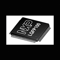
XA-H3 NXP Semiconductors, XA-H3 Datasheet - Page 28

XA-H3
Manufacturer Part Number
XA-H3
Description
The powerful 16-bit XA CPU core and rich feature set make the XA-H3 and XA-H4 devices ideal for high-performance real-time applications such as industrial control and networking
Manufacturer
NXP Semiconductors
Datasheet
1.XA-H3.pdf
(36 pages)
1. On a 16-bit bus, if only one byte is being written, then only one of BLE or BHE will go active. On an 8-bit bus, BLE goes active for all (odd or
2. The bus timing is designed to make meeting hold time very straightforward without glue logic. On all reads and fetches, in order to meet hold
3. To avoid 3-State fights during read cycles and fetch cycles, do not drive data bus until OE goes active
4. WARNING: ClkOut is specified at 40 pF max. More than 40 pf on ClkOut may significantly degrade the ClkOut waveform. Load capacitance
5. Not all combinations of bus timing configuration values result in valid bus cycles. Please refer to the XA-H3 User Manual for details.
6. When code is being fetched on the external bus, a burst mode fetch is used. This burst can be from 2 to 16 bytes long. On a 16-bit bus,
7. The MIN value for this parameter is guaranteed by design and is not tested in production to the specified limit. In those cases where a
Philips Semiconductors
PRELIMINARY AC ELECTRICAL CHARACTERISTICS (5.0 V +/–10%)
NOTE:
1999 Sep 24
Symbol
Symbol
CMOS 16-bit highly integrated microcontroller
t
t
t
t
t
t
t
t
t
even address) accesses. BHE will not go active during any accesses on an 8 bit bus.
time, the slave should hold data valid on the bus until the earliest of CS, BHE/BLE, OE, goes high (inactive), or until the address changes.
for all outputs (except ClkOut) = 80 pF.
A3 – A1 are incremented for each new word of the burst. On an 8-bit bus, A3 – A0 are incremented for each new byte of the burst code fetch.
maximum value is specified in the table for this parameter, it is tested.
t
t
t
t
t
t
t
CHCX
CHAH
CHSH
CODH
AHDR
OHDE
CHDV
SHDH
CLCX
CLCH
CHCL
CHAV
CHSL
SHAH
AVSL
DVSL
t
t
t
t
F
DIS
DIH
WH
WS
t
C
C
7, 8, 10, 11
7, 8, 10, 11
Fig re
Figure
9, 12
9, 12
13
13
13
13
13
All
All
All
All
All
14
10
10
12
15
15
9
System Clock Frequency
System Clock Period = 1/FC
XTALIN High Time
XTALIN Low Time
XTALIN Rise Time
XTALIN Fall Time
Address Valid to Strobe low
Address hold after CLKOUT rising edge
Delay from CLKOUT rising edge to address valid
Delay from CLKOUT rising edge to Strobe High
Delay from CLKOUT rising edge to Strobe Low
ClkOut Duty Cycle High (into 40 pF max.)
Address hold (A19 – A1 only, not A0) after CS, BLE, BHE rise at end
of Data Read Cycle (not code fetch)
Data In Valid setup to ClkOut rising edge
Data In Valid hold after ClkOut rising edge
OE high to XA Data Bus Driver Enable
Clock High to Data Valid
Data Valid prior to Strobe Low
Minimum Address Hold Time after strobe goes inactive
Data hold after strobes (CS and BHE/BLE) high
WAIT setup (stable high or low) to CLKOUT rising edge
WAIT hold (stable high or low) after CLKOUT rising edge
Data Read and Instruction Fetch Cycles
Data Read Only
Parameter
Parameter
Write Cycles
All Cycles
Wait Input
28
7
2
7
7
t
t
t
t
t
t
t
t
t
CHCX
33.33
C
C
C
C
C
C
C
C
Min
* 0.5
* 0.4
25
20
– 21
– 12
– 14
– 23
– 25
– 25
0
–
–
1
–
1
1
0
–
0
–7
Limits
Preliminary specification
t
CHCX
Max
30
25
21
19
25
–
–
–
5
5
–
–
–
–
–
–
–
–
–
–
–
XA-H3
+3
Unit
Unit
MHz
ns
ns
ns
ns
ns
ns
ns
ns
ns
ns
ns
ns
ns
ns
ns
ns
ns
ns
ns
ns
ns


