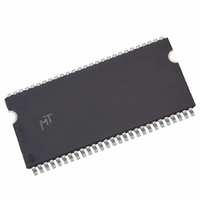
MT48LC8M16A2P-75:G Micron Technology Inc, MT48LC8M16A2P-75:G Datasheet - Page 16

MT48LC8M16A2P-75:G
Manufacturer Part Number
MT48LC8M16A2P-75:G
Description
IC SDRAM 128MBIT 133MHZ 54TSOP
Manufacturer
Micron Technology Inc
Type
SDRAMr
Specifications of MT48LC8M16A2P-75:G
Memory Type
SDRAM
Format - Memory
RAM
Memory Size
128M (8Mx16)
Speed
133MHz
Interface
Parallel
Voltage - Supply
3 V ~ 3.6 V
Operating Temperature
0°C ~ 70°C
Package / Case
54-TSOP II
Memory Configuration
16M X 8
Access Time
5.4ns
Page Size
128Mbit
Memory Case Style
TSOP
No. Of Pins
54
Operating Temperature Range
0°C To +70°C
Organization
8Mx16
Density
128Mb
Address Bus
14b
Access Time (max)
6/5.4ns
Maximum Clock Rate
133MHz
Operating Supply Voltage (typ)
3.3V
Package Type
TSOP-II
Operating Temp Range
0C to 70C
Operating Supply Voltage (max)
3.6V
Operating Supply Voltage (min)
3V
Supply Current
150mA
Pin Count
54
Mounting
Surface Mount
Operating Temperature Classification
Commercial
Lead Free Status / RoHS Status
Lead free / RoHS Compliant
Lead Free Status / RoHS Status
Compliant, Lead free / RoHS Compliant
Available stocks
Company
Part Number
Manufacturer
Quantity
Price
Company:
Part Number:
MT48LC8M16A2P-75:G
Manufacturer:
MICRON
Quantity:
8
Part Number:
MT48LC8M16A2P-75:G
Manufacturer:
MICRON
Quantity:
20 000
Register Definition
Mode Register
Burst Length (BL)
PDF: 09005aef8091e66d/Source: 09005aef8091e625
128MSDRAM_2.fm - Rev. N 1/09 EN
Note:
10. Issue an AUTO REFRESH command.
11. Wait at least
12. The SDRAM is now ready for mode register programming. Because the mode register
13. Wait at least
7. Wait at least
8. Issue an AUTO REFRESH command.
9. Wait at least
At this point, the DRAM is ready for any valid command.
The mode register is used to define the specific mode of operation of the SDRAM. This
definition includes the selection of a burst length (BL), a burst type, a CAS latency (CL),
an operating mode, and a write burst mode, as shown in Figure 7 on page 18. The mode
register is programmed via the LMR command and will retain the stored information
until it is programmed again or the device loses power.
Mode register bits M0–M2 specify the BL, M3 specifies the type of burst (sequential or
interleaved), M4–M6 specify the CL, M7 and M8 specify the operating mode, M9 speci-
fies the write burst mode, and M10 and M11 are reserved for future use.
The mode register must be loaded when all banks are idle, and the controller must wait
the specified time before initiating the subsequent operation. Violating either of these
requirements will result in unspecified operation.
Read and write accesses to the SDRAM are burst oriented, with the BL being program-
mable, as shown in Figure 7 on page 18. BL determines the maximum number of
column locations that can be accessed for a given READ or WRITE command. BL of 1, 2,
4, or 8 locations are available for both the sequential and the interleaved burst types, and
a full-page burst is available for the sequential mode. The full-page burst is used in
conjunction with the BURST TERMINATE command to generate arbitrary BLs.
Reserved states cannot be used because unknown operation or incompatibility with
future versions may result.
given. All banks will complete their precharge, thereby placing the device in the all
banks idle state.
are allowed.
are allowed.
will power up in an unknown state, it should be loaded with desired bit values prior to
applying any operational command. Using the LMR command, program the mode
register. The mode register is programmed via the MODE REGISTER SET command
with BA1 = 0, BA0 = 0 and retains the stored information until it is programmed again
or the device loses power. Not programming the mode register upon initialization will
result in default settings, which may not be desired. Outputs are guaranteed High-Z
after the LMR command is issued. Outputs should be High-Z already before the LMR
command is issued.
allowed.
If desired, more than two AUTO REFRESH commands can be issued in the sequence.
After steps 9 and 10 are complete, repeat them until the desired number of AUTO
REFRESH +
t
t
t
t
t
RFC loops is achieved.
RP time; during this time, NOPs or DESELECT commands must be
RFC time, during which only NOPs or COMMAND INHIBIT commands
RFC time, during which only NOPs or COMMAND INHIBIT commands
MRD time, during which only NOP or DESELECT commands are
16
Micron Technology, Inc., reserves the right to change products or specifications without notice.
128Mb: x4, x8, x16 SDRAM
Functional Description
©1999 Micron Technology, Inc. All rights reserved.


