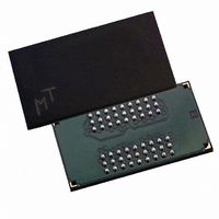
MT48V8M16LFB4-8:G Micron Technology Inc, MT48V8M16LFB4-8:G Datasheet - Page 21

MT48V8M16LFB4-8:G
Manufacturer Part Number
MT48V8M16LFB4-8:G
Description
IC SDRAM 128MBIT 125MHZ 54VFBGA
Manufacturer
Micron Technology Inc
Type
Mobile SDRAMr
Specifications of MT48V8M16LFB4-8:G
Format - Memory
RAM
Memory Type
Mobile SDRAM
Memory Size
128M (8Mx16)
Speed
125MHz
Interface
Parallel
Voltage - Supply
2.3 V ~ 2.7 V
Operating Temperature
0°C ~ 70°C
Package / Case
54-VFBGA
Organization
8Mx16
Density
128Mb
Address Bus
14b
Access Time (max)
19/8/7ns
Maximum Clock Rate
125MHz
Operating Supply Voltage (typ)
2.5V
Package Type
VFBGA
Operating Temp Range
0C to 70C
Operating Supply Voltage (max)
2.7V
Operating Supply Voltage (min)
2.3V
Supply Current
100mA
Pin Count
54
Mounting
Surface Mount
Operating Temperature Classification
Commercial
Lead Free Status / RoHS Status
Lead free / RoHS Compliant
Available stocks
Company
Part Number
Manufacturer
Quantity
Price
Company:
Part Number:
MT48V8M16LFB4-8:G
Manufacturer:
MICRON
Quantity:
4 000
Company:
Part Number:
MT48V8M16LFB4-8:G
Manufacturer:
Micron Technology Inc
Quantity:
10 000
Company:
Part Number:
MT48V8M16LFB4-8:G TR
Manufacturer:
Micron Technology Inc
Quantity:
10 000
Operating Mode
Extended Mode Register
Figure 9:
Temperature-Compensated Self Refresh (TCSR)
PDF: 09005aef807f4885/Source: 09005aef8071a76b
128Mbx16x32Mobile_2.fm - Rev. M 1/09 EN
E13
E11
0
0
1
1
0
–
E12
E10
0
1
0
1
0
–
Extended Mode Register
Mode Register Definition
Mode Register
Reserved
Extended Mode
Resereved
E9
0
–
Notes:
E8
0
–
E7
0
–
Register
The normal operating mode is selected by setting M7, M8, M10, and M11 to zero; all the
other combinations of values for M7, M8, M10, and M11 are reserved for future use and/
or test modes.
Test modes and reserved states should not be used because unknown operation or
incompatibility with future versions may result.
The extended mode register controls the functions beyond those controlled by the mode
register. These additional functions are special features of the Mobile device. They
include TCSR and PASR.
1. E13 and E12 (BA1 and BA0) must be “1, 0” to select the extended mode register (vs. the
2. RFU: reserved for future use.
The extended mode register is programmed via the MODE REGISTER SET command
(BA1 = 1, BA0 = 0) and retains the stored information until it is programmed again or the
device loses power.
The extended mode register must be programmed with E5 through E11 set to “0.” The
extended mode register must be loaded when all banks are idle and no bursts are in
progress, and the controller must wait the specified time before initiating any subse-
quent operation. Violating either of these requirements results in unspecified operation.
The extended mode register must be programmed to ensure proper operation.
TCSR allows the controller to program the refresh interval during self refresh mode,
according to the case temperature of the Mobile device. This allows great power savings
during self refresh during most operating temperature ranges. Only during extreme
temperatures would the controller have to select a higher TCSR level that will guarantee
data during self refresh.
E6
0
–
base mode register).
E5
0
–
BA1 BA0
E13 E12
13
EMR
E4 E3 E2 E1 E0
12
A11
11
Valid
E11
–
Maximum Case Temp.
10
A10
E10
9
set to “0”
A9
E9
All other states reserved
8
A8
E8
Operating Mode
Normal Operation
7
A7
E7
85°C
70°C
45°C
15°C
6
A6
E6
21
5
A5
E5
E4
TCSR
1
0
0
1
4
A4
E4
3
E3
A3
E3
1
0
1
0
2
A2
Micron Technology, Inc., reserves the right to change products or specifications without notice.
E2
PASR
Partial-Array Self Refresh Coverage
1
A1
E1
0
A0
E0
Quarter Array (BA1 = BA0 = 0)
128Mb: x16, x32 Mobile SDRAM
Extended Mode
Register (Ex)
FullArray (All Banks)
Half Array (BA1 = 0)
©2001 Micron Technology, Inc. All rights reserved.
Register Definition
RFU
RFU
RFU
RFU
RFU
E2
0
0
0
0
1
1
1
1
E1
0
0
1
1
0
0
1
1
E0
0
1
0
1
0
1
0
1


