MT48V8M16LFB4-8:G Micron Technology Inc, MT48V8M16LFB4-8:G Datasheet - Page 6
MT48V8M16LFB4-8:G
Manufacturer Part Number
MT48V8M16LFB4-8:G
Description
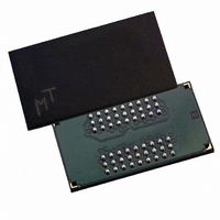
IC SDRAM 128MBIT 125MHZ 54VFBGA
Manufacturer
Micron Technology Inc
Type
Mobile SDRAMr
Specifications of MT48V8M16LFB4-8:G
Format - Memory
RAM
Memory Type
Mobile SDRAM
Memory Size
128M (8Mx16)
Speed
125MHz
Interface
Parallel
Voltage - Supply
2.3 V ~ 2.7 V
Operating Temperature
0°C ~ 70°C
Package / Case
54-VFBGA
Organization
8Mx16
Density
128Mb
Address Bus
14b
Access Time (max)
19/8/7ns
Maximum Clock Rate
125MHz
Operating Supply Voltage (typ)
2.5V
Package Type
VFBGA
Operating Temp Range
0C to 70C
Operating Supply Voltage (max)
2.7V
Operating Supply Voltage (min)
2.3V
Supply Current
100mA
Pin Count
54
Mounting
Surface Mount
Operating Temperature Classification
Commercial
Lead Free Status / RoHS Status
Lead free / RoHS Compliant
Available stocks
Company
Part Number
Manufacturer
Quantity
Price
Company:

Part Number:
MT48V8M16LFB4-8:G
Manufacturer:
MICRON
Quantity:
4 000
Company:
Part Number:
MT48V8M16LFB4-8:G
Manufacturer:
Micron Technology Inc
Quantity:
10 000
Company:
Part Number:
MT48V8M16LFB4-8:G TR
Manufacturer:
Micron Technology Inc
Quantity:
10 000


Figure 1:
FBGA Part Marking Decoder
General Description
PDF: 09005aef807f4885/Source: 09005aef8071a76b
128Mbx16x32Mobile_2.fm - Rev. M 1/09 EN
128Mb SDRAM Part Numbers
Notes:
1. Not all speeds and configurations are available.
2. Contact Micron for availability.
Due to space limitations, FBGA-packaged components have an abbreviated part
marking that is different from the part number. Micron’s new FBGA Part Marking
Decoder makes it easier to understand that part marking. Visit the Web site at
www.micron.com/decoder.
The Micron
memory containing 134,217,728 bits. It is internally configured as a quad-bank DRAM
with a synchronous interface (all signals are registered on the positive edge of the clock
signal, CLK). Each of the x16’s 33,554,432-bit banks is organized as 4,096 rows by 512
columns by 16 bits. Each of the x32’s 33,554,432-bit banks is organized as 4,096 rows by
256 columns by 32 bits.
Read and write accesses to the SDRAM are burst oriented; accesses start at a selected
location and continue for a programmed number of locations in a programmed
sequence. Accesses begin with the registration of an ACTIVE command, which is then
followed by a READ or WRITE command. The address bits registered coincident with the
ACTIVE command are used to select the bank and row to be accessed (BA0, BA1 select
the bank; A0–A11 select the row). The address bits registered coincident with the READ
or WRITE command are used to select the starting column location for the burst access.
The SDRAM provides for programmable read or write burst lengths (BL) of 1, 2, 4, or 8
locations, or the full page, with a burst terminate option. An auto precharge function
may be enabled to provide a self-timed row precharge that is initiated at the end of the
burst sequence.
Voltage (V
3.3V/ 3.3V
2.5V / 2.5V–1.8V
90-ball VFBGA (8 x 13mm) lead-free
Configuration
8 Meg x 16
4 Meg x 32
90-ball VFBGA (8 x 13mm)
54-pin TSOP II (400 mil)
Package
54-ball VFBGA (8 x 8mm)
54-ball VFBGA (8 x 8mm) lead-free
54-pin TSOP II (400 mil) Lead-Free
MT4 8
DD
/V
Example Part Number: MT48V4M32LFF5-10XT
DD
®
Q)
128Mb SDRAM device is a high-speed CMOS, dynamic random access
V
V
8M16
4M32
DD
DD
LC
V
/
Q
Configuration
F4
B4
F5
B5
TG
P
6
2
2
L F
Micron Technology, Inc., reserves the right to change products or specifications without notice.
Package
-
128Mb: x16, x32 Mobile SDRAM
Speed
FBGA Part Marking Decoder
-75M
-10
T emperature
AT
IT
-8
2
2
Speed Grade
t
t
t
CK = 7.5ns, CL = 3
CK = 8ns, CL = 3
CK = 10ns, CL = 3
Operating T emp
:G
©2001 Micron Technology, Inc. All rights reserved.
Automotive
Industrial
Standard
Revision
Revision
Rev
Related parts for MT48V8M16LFB4-8:G
Image
Part Number
Description
Manufacturer
Datasheet
Request
R

Part Number:
Description:
IC SDRAM 64MBIT 133MHZ 54TSOP
Manufacturer:
Micron Technology Inc
Datasheet:

Part Number:
Description:
IC SDRAM 64MBIT 5.5NS 86TSOP
Manufacturer:
Micron Technology Inc
Datasheet:
Part Number:
Description:
IC SDRAM 64MBIT 200MHZ 86TSOP
Manufacturer:
Micron Technology Inc
Datasheet:
Part Number:
Description:
IC SDRAM 64MBIT 133MHZ 54TSOP
Manufacturer:
Micron Technology Inc
Datasheet:
Part Number:
Description:
IC SDRAM 128MBIT 133MHZ 54TSOP
Manufacturer:
Micron Technology Inc
Datasheet:

Part Number:
Description:
IC SDRAM 256MBIT 133MHZ 90VFBGA
Manufacturer:
Micron Technology Inc
Datasheet:
Part Number:
Description:
IC SDRAM 128MBIT 133MHZ 54TSOP
Manufacturer:
Micron Technology Inc
Datasheet:
Part Number:
Description:
IC SDRAM 256MBIT 133MHZ 54TSOP
Manufacturer:
Micron Technology Inc
Datasheet:

Part Number:
Description:
IC DDR SDRAM 512MBIT 6NS 66TSOP
Manufacturer:
Micron Technology Inc
Datasheet:
Part Number:
Description:
IC SDRAM 128MBIT 167MHZ 86TSOP
Manufacturer:
Micron Technology Inc
Datasheet:
Part Number:
Description:
IC SDRAM 128MBIT 143MHZ 86TSOP
Manufacturer:
Micron Technology Inc
Datasheet:

Part Number:
Description:
SDRAM 256M-BIT 1.8V 54-PIN VFBGA
Manufacturer:
Micron Technology Inc
Datasheet:
Part Number:
Description:
IC SDRAM 128MBIT 143MHZ 86TSOP
Manufacturer:
Micron Technology Inc
Datasheet:

Part Number:
Description:
IC SDRAM 128MBIT 125MHZ 54VFBGA
Manufacturer:
Micron Technology Inc
Datasheet:
Part Number:
Description:
IC PSRAM 64MB 54-VFBGA
Manufacturer:
Micron Technology Inc
Datasheet: