CP2400DK Silicon Laboratories Inc, CP2400DK Datasheet - Page 16
CP2400DK
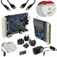
Manufacturer Part Number
CP2400DK
Description
KIT EVAL SPI LCD DRIVER CP2400
Manufacturer
Silicon Laboratories Inc
Specifications of CP2400DK
Main Purpose
LCD Development
Embedded
Yes
Utilized Ic / Part
CP2400
Primary Attributes
I²C, SMBus Interfaces
Secondary Attributes
Up to 128 segments
Product
Microcontroller Modules
Core Processor
C8051F930
Clock Speed
20 MHz
Interface Type
SPI
Timers
2
Operating Supply Voltage
1.8 V to 3.6 V
Cpu Core
C8051F930
Lead Free Status / RoHS Status
Contains lead / RoHS non-compliant
Lead Free Status / RoHS Status
Lead free / RoHS Compliant, Contains lead / RoHS non-compliant
Other names
336-1858
336-1858
336-1858


CP2400/1/2/3
Table 3.4. Power Management Electrical Specifications
V
Table 3.5. Internal Oscillator Electrical Characteristics
V
Table 3.6. LCD Electrical Characteristics
V
16
Table 3.3. Reset Electrical Characteristics
V
RAM Preservation Mode Wake-Up
Time
ULP Mode Wake-Up Time (from
the falling edge of NSS/PWR to
the reset complete interrupt)
Oscillator Frequency
Oscillator Supply Current (from V
Parameter
Charge Pump Output Voltage Error
RST Input High Voltage
RST Input Low Voltage
RST Input Pullup Current
V
Power on Reset Delay (T
from Start of Ramp until the Reset
Complete Interrupt
Required RST Low Time to
guarantee a System Reset (T
Startup Delay from Reset De-
asserted until the Reset Complete
Interrupt (T
Notes:
DD
DD
DD
DD
DD
1. There is no restriction on VDD ramp time if the RST pin is toggled at the end of the ramp.
2. If the
= 1.8 to 3.6 V, –40 to +85 °C unless otherwise specified.
= 1.8 to 3.6 V; T
= 1.8 to 3.6 V; T
= 1.8 to 3.6 V, –40 to +85 °C unless otherwise specified.
Ramp Time for Power On
STARTUP
RST pin is held low for a shorter time period, a device reset may occur.
Parameter
Parameters
Parameter
A
A
= –40 to +85 °C unless otherwise specified; Using factory-calibrated settings.
= –40 to +85 °C unless otherwise specified.
)
PORDelay
RST
1
DD
)
)
)
From the falling edge of CLK until
host interface ready
Port Match or SmaRTClock Wakeup
NSS/PWR Pin Wakeup
V
RST = 0 V, V
RST = 0 V, V
DD
Ramp from 0–1.8 V
V
V
V
V
Conditions
See Note 2
–40 to +85 °C,
Pin Reset
DD
DD
DD
DD
Conditions
Conditions
Rev. 1.0
Conditions
= 1.8–3.6 V
= 1.8 V
= 3.0 V
= 3.6 V
25 °C
DD
DD
= 1.8 V
= 3.6 V
0.7 x V
Min
15
—
—
—
—
—
—
—
—
Min
15
—
DD
Min
Min
3
7
—
1200
Typ
660
575
Typ
20
90
—
—
—
—
20
50
4
Typ
Typ
±30
10
—
—
0.3 x V
Max
25
Max
—
Max
900
100
Max
30
—
—
—
—
—
—
1
4
8
DD
Units
Units
UNITS
Cycles
MHz
Units
mV
RTC
µA
µA
ms
µs
µs
µs
ns
V
V
Related parts for CP2400DK
Image
Part Number
Description
Manufacturer
Datasheet
Request
R

Part Number:
Description:
IC LCD DRIVER 48TQFP
Manufacturer:
Silicon Laboratories Inc
Datasheet:
Part Number:
Description:
IC LCD DRIVER 48QFN
Manufacturer:
Silicon Laboratories Inc
Datasheet:

Part Number:
Description:
SMD/C°/SINGLE-ENDED OUTPUT SILICON OSCILLATOR
Manufacturer:
Silicon Laboratories Inc
Part Number:
Description:
Manufacturer:
Silicon Laboratories Inc
Datasheet:
Part Number:
Description:
N/A N/A/SI4010 AES KEYFOB DEMO WITH LCD RX
Manufacturer:
Silicon Laboratories Inc
Datasheet:
Part Number:
Description:
N/A N/A/SI4010 SIMPLIFIED KEY FOB DEMO WITH LED RX
Manufacturer:
Silicon Laboratories Inc
Datasheet:
Part Number:
Description:
N/A/-40 TO 85 OC/EZLINK MODULE; F930/4432 HIGH BAND (REV E/B1)
Manufacturer:
Silicon Laboratories Inc
Part Number:
Description:
EZLink Module; F930/4432 Low Band (rev e/B1)
Manufacturer:
Silicon Laboratories Inc
Part Number:
Description:
I°/4460 10 DBM RADIO TEST CARD 434 MHZ
Manufacturer:
Silicon Laboratories Inc
Part Number:
Description:
I°/4461 14 DBM RADIO TEST CARD 868 MHZ
Manufacturer:
Silicon Laboratories Inc
Part Number:
Description:
I°/4463 20 DBM RFSWITCH RADIO TEST CARD 460 MHZ
Manufacturer:
Silicon Laboratories Inc
Part Number:
Description:
I°/4463 20 DBM RADIO TEST CARD 868 MHZ
Manufacturer:
Silicon Laboratories Inc
Part Number:
Description:
I°/4463 27 DBM RADIO TEST CARD 868 MHZ
Manufacturer:
Silicon Laboratories Inc
Part Number:
Description:
I°/4463 SKYWORKS 30 DBM RADIO TEST CARD 915 MHZ
Manufacturer:
Silicon Laboratories Inc