CP2400DK Silicon Laboratories Inc, CP2400DK Datasheet - Page 61
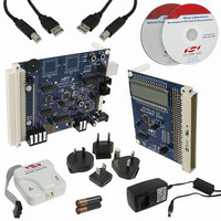
CP2400DK
Manufacturer Part Number
CP2400DK
Description
KIT EVAL SPI LCD DRIVER CP2400
Manufacturer
Silicon Laboratories Inc
Specifications of CP2400DK
Main Purpose
LCD Development
Embedded
Yes
Utilized Ic / Part
CP2400
Primary Attributes
I²C, SMBus Interfaces
Secondary Attributes
Up to 128 segments
Product
Microcontroller Modules
Core Processor
C8051F930
Clock Speed
20 MHz
Interface Type
SPI
Timers
2
Operating Supply Voltage
1.8 V to 3.6 V
Cpu Core
C8051F930
Lead Free Status / RoHS Status
Contains lead / RoHS non-compliant
Lead Free Status / RoHS Status
Lead free / RoHS Compliant, Contains lead / RoHS non-compliant
Other names
336-1858
336-1858
336-1858


10.1. Port I/O Modes of Operation
All port pins use the Port I/O cell shown in Figure 10.2. Each Port I/O cell can be configured by software for analog
I/O or digital I/O using the PnMDI registers. On reset or wake-up from ULP mode, all Port I/O cells default to a
digital high impedance state with weak pull-ups enabled.
10.1.1. Port Pins Configured for Analog I/O
Any pins to be used for LCD should be configured for analog I/O (PnMDI.n = 0). When a pin is configured for
analog I/O, its weak pullup and digital output driver and receiver are disabled. Port pins configured for analog I/O
will always read back a value of 0 regardless of the actual voltage on the pin.
10.1.2. Port Pins Configured For Digital I/O
Any pins to be used for GPIO or Port Match should be configured as digital I/O (PnMDI.n = 1). For digital I/O pins,
one of two output modes (push-pull or open-drain) must be selected using the PnMDO registers.
Push-pull outputs (PnMDO.n = 1) always drive the Port pad to the V
logic value of the Port pin. Open-drain outputs have the high side driver disabled; therefore, they only drive the Port
pad to GND when the output logic value is 0 and become high impedance inputs (both high and low drivers turned
off) when the output logic value is 1.
When a digital I/O cell is placed in the high impedance state, a weak pull-up transistor pulls the Port pad to the VDD
supply voltage to ensure the digital input is at a defined logic state. Weak pullups are disabled when the I/O cell is
driven to GND to minimize power consumption. The user must ensure that digital I/O are always internally or
externally pulled or driven to a valid logic state. An analog signal applied to a digital I/O pin will result in increased
power consumption.
PxOUT.x – Output
Logic Value
(Port Latch)
PxMDO.x
(1 for push-pull)
(0 for open-drain)
PxIN.x – Input Logic Value
(Reads 0 when pin is configured as an analog I/O)
To/From Analog
Peripheral
PxMDI.x
(1 for digital)
(0 for analog)
Figure 10.2. Port I/O Cell Block Diagram
Rev. 1.0
DD
VDD
GND
or GND supply rails based on the output
VDD
CP2400/1/2/3
(WEAK)
PORT
PAD
61
Related parts for CP2400DK
Image
Part Number
Description
Manufacturer
Datasheet
Request
R

Part Number:
Description:
IC LCD DRIVER 48TQFP
Manufacturer:
Silicon Laboratories Inc
Datasheet:
Part Number:
Description:
IC LCD DRIVER 48QFN
Manufacturer:
Silicon Laboratories Inc
Datasheet:

Part Number:
Description:
SMD/C°/SINGLE-ENDED OUTPUT SILICON OSCILLATOR
Manufacturer:
Silicon Laboratories Inc
Part Number:
Description:
Manufacturer:
Silicon Laboratories Inc
Datasheet:
Part Number:
Description:
N/A N/A/SI4010 AES KEYFOB DEMO WITH LCD RX
Manufacturer:
Silicon Laboratories Inc
Datasheet:
Part Number:
Description:
N/A N/A/SI4010 SIMPLIFIED KEY FOB DEMO WITH LED RX
Manufacturer:
Silicon Laboratories Inc
Datasheet:
Part Number:
Description:
N/A/-40 TO 85 OC/EZLINK MODULE; F930/4432 HIGH BAND (REV E/B1)
Manufacturer:
Silicon Laboratories Inc
Part Number:
Description:
EZLink Module; F930/4432 Low Band (rev e/B1)
Manufacturer:
Silicon Laboratories Inc
Part Number:
Description:
I°/4460 10 DBM RADIO TEST CARD 434 MHZ
Manufacturer:
Silicon Laboratories Inc
Part Number:
Description:
I°/4461 14 DBM RADIO TEST CARD 868 MHZ
Manufacturer:
Silicon Laboratories Inc
Part Number:
Description:
I°/4463 20 DBM RFSWITCH RADIO TEST CARD 460 MHZ
Manufacturer:
Silicon Laboratories Inc
Part Number:
Description:
I°/4463 20 DBM RADIO TEST CARD 868 MHZ
Manufacturer:
Silicon Laboratories Inc
Part Number:
Description:
I°/4463 27 DBM RADIO TEST CARD 868 MHZ
Manufacturer:
Silicon Laboratories Inc
Part Number:
Description:
I°/4463 SKYWORKS 30 DBM RADIO TEST CARD 915 MHZ
Manufacturer:
Silicon Laboratories Inc