CP2400DK Silicon Laboratories Inc, CP2400DK Datasheet - Page 36
CP2400DK
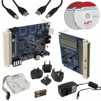
Manufacturer Part Number
CP2400DK
Description
KIT EVAL SPI LCD DRIVER CP2400
Manufacturer
Silicon Laboratories Inc
Specifications of CP2400DK
Main Purpose
LCD Development
Embedded
Yes
Utilized Ic / Part
CP2400
Primary Attributes
I²C, SMBus Interfaces
Secondary Attributes
Up to 128 segments
Product
Microcontroller Modules
Core Processor
C8051F930
Clock Speed
20 MHz
Interface Type
SPI
Timers
2
Operating Supply Voltage
1.8 V to 3.6 V
Cpu Core
C8051F930
Lead Free Status / RoHS Status
Contains lead / RoHS non-compliant
Lead Free Status / RoHS Status
Lead free / RoHS Compliant, Contains lead / RoHS non-compliant
Other names
336-1858
336-1858
336-1858


CP2400/1/2/3
6.2.
The SMBus interface supports 6 commands which provide access to all internal registers and RAM. The six
commands are listed in Table 6.2. Detailed information on the SMBus interface including bus timing can be found in
Section “15. SMBus Interface” on page 104.
Figure 6.3 shows typical SMBus read and write transfers used to access internal registers or RAM. The first three
bytes of a write transfer are interpreted as COMMAND, ADDRH, and ADDRL. For the REGPOLL, REGREAD, and
RAMREAD commands, a repeated start is required to begin data transfer. The host controller may also choose to
end the transfer with a STOP and then start a new read transfer using the same setup information. For the WRITE
and RAMWRITE command, an SMBus write transfer is required. Starting with the fourth byte following the slave
address, all bytes written are interpreted as data. The SMBus transfer ends when the host sends a STOP.
Note: Using the RAMREAD command to read an address outside the 0x400–0x4FF range will result in a data value of 0xDE.
36
REGPOLL
REGREAD
REGSET
REGWRITE
RAMREAD
RAMWRITE
Accessing Internal Registers and RAM over the SMBus Interface
SMBus Read (Data Transfer):
Command
SMBus Read (Setup):
SMBus Write:
S
S
R
S
SLA
SLA
SLA
W
W
R
Received by
CP240x
Transmitted by
CP240x
A
A
A
OPCODE
COMMAND
COMMAND
0x01
0x02
0x03
0x06
0x08
Data 0
0x04
Table 6.2. SMBus Command Set
A
Figure 6.3. SMBus Transfers
Writes one or more bytes to a single register. Used for generating a
A
A
Reads one or more bytes from registers with sequential addresses.
waveform on a GPIO pin or updating the SmaRTClock registers.
Writes one or more bytes to registers with sequential addresses.
Reads data from a single register. Used for polling a status bit.
ADDRH
ADDRH
Reads one or more bytes from sequential RAM locations.
S = START
R = REPEATED START
P = STOP
A = ACK
N = NACK
Writes one or more bytes to sequential RAM locations.
Data N
Rev. 1.0
A
A
N
ADDRL
ADDRL
P
A
A
Description
Data 0
+ Data Transfer or STOP
R = READ
W = WRITE
SLA = Slave Address
A
Data N
A
P
Related parts for CP2400DK
Image
Part Number
Description
Manufacturer
Datasheet
Request
R

Part Number:
Description:
IC LCD DRIVER 48TQFP
Manufacturer:
Silicon Laboratories Inc
Datasheet:
Part Number:
Description:
IC LCD DRIVER 48QFN
Manufacturer:
Silicon Laboratories Inc
Datasheet:

Part Number:
Description:
SMD/C°/SINGLE-ENDED OUTPUT SILICON OSCILLATOR
Manufacturer:
Silicon Laboratories Inc
Part Number:
Description:
Manufacturer:
Silicon Laboratories Inc
Datasheet:
Part Number:
Description:
N/A N/A/SI4010 AES KEYFOB DEMO WITH LCD RX
Manufacturer:
Silicon Laboratories Inc
Datasheet:
Part Number:
Description:
N/A N/A/SI4010 SIMPLIFIED KEY FOB DEMO WITH LED RX
Manufacturer:
Silicon Laboratories Inc
Datasheet:
Part Number:
Description:
N/A/-40 TO 85 OC/EZLINK MODULE; F930/4432 HIGH BAND (REV E/B1)
Manufacturer:
Silicon Laboratories Inc
Part Number:
Description:
EZLink Module; F930/4432 Low Band (rev e/B1)
Manufacturer:
Silicon Laboratories Inc
Part Number:
Description:
I°/4460 10 DBM RADIO TEST CARD 434 MHZ
Manufacturer:
Silicon Laboratories Inc
Part Number:
Description:
I°/4461 14 DBM RADIO TEST CARD 868 MHZ
Manufacturer:
Silicon Laboratories Inc
Part Number:
Description:
I°/4463 20 DBM RFSWITCH RADIO TEST CARD 460 MHZ
Manufacturer:
Silicon Laboratories Inc
Part Number:
Description:
I°/4463 20 DBM RADIO TEST CARD 868 MHZ
Manufacturer:
Silicon Laboratories Inc
Part Number:
Description:
I°/4463 27 DBM RADIO TEST CARD 868 MHZ
Manufacturer:
Silicon Laboratories Inc
Part Number:
Description:
I°/4463 SKYWORKS 30 DBM RADIO TEST CARD 915 MHZ
Manufacturer:
Silicon Laboratories Inc