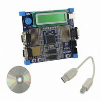
OM11014 NXP Semiconductors, OM11014 Datasheet - Page 18

OM11014
Manufacturer Part Number
OM11014
Description
BOARD EVAL FOR LPC2919
Manufacturer
NXP Semiconductors
Series
Keilr
Type
MCUr
Datasheet
1.OM11014.pdf
(67 pages)
Specifications of OM11014
Contents
Board, Cable, CD
For Use With/related Products
LPC2919
Lead Free Status / RoHS Status
Not applicable / Not applicable
Other names
568-4360
NXP Semiconductors
LPC2917_19_1
Product data sheet
8.2.2 Description
The SMC simultaneously supports up to eight independently configurable memory banks.
Each memory bank can be 8 bits, 16 bits or 32 bits wide and is capable of supporting
SRAM, ROM, burst-ROM memory or external I/O devices.
A separate chip select output is available for each bank. The chip select lines are
configurable to be active HIGH or LOW. Memory-bank selection is controlled by memory
addressing.
memory base addresses, chip selects and bank internal addresses.
Table 10.
Table 11.
32-bit
system
address bit
field
31 to 29
28 to 26
25 and 24
23 to 0
CS[2:0]
000
001
010
011
100
101
110
111
•
•
•
•
•
•
•
•
•
•
Asynchronous page-mode read operation in non-clocked memory subsystems
Asynchronous burst-mode read access to burst-mode ROM devices
Independent configuration for up to eight banks, each up to 16 MB
Programmable bus-turnaround (idle) cycles (one to 16)
Programmable read and write wait states (up to 32), for static RAM devices
Programmable initial and subsequent burst-read wait state for burst-ROM devices
Programmable write protection
Programmable burst-mode operation
Programmable external data width: 8 bits, 16 bits or 32 bits
Programmable read-byte lane enable control
External memory-bank address bit description
External static-memory controller banks
Table 10
Symbol
BA[2:0]
CS[2:0]
-
A[23:0]
Bank
bank 0
bank 1
bank 2
bank 3
bank 4
bank 5
bank 6
bank 7
shows how the 32-bit system address is mapped to the external bus
Rev. 01 — 31 July 2008
Description
external static-memory base address (three most significant bits);
the base address can be found in the memory map; see
field contains ‘010’ when addressing an external memory bank.
chip select address space for eight memory banks; see
always ‘00’; other values are ‘mirrors’ of the 16 MB bank address
16 MB memory banks address space
ARM9 microcontroller with CAN and LIN
LPC2917/19
© NXP B.V. 2008. All rights reserved.
Ref.
[1]
1. This
18 of 67


