OM11014 NXP Semiconductors, OM11014 Datasheet - Page 55
OM11014
Manufacturer Part Number
OM11014
Description
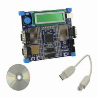
BOARD EVAL FOR LPC2919
Manufacturer
NXP Semiconductors
Series
Keilr
Type
MCUr
Datasheet
1.OM11014.pdf
(67 pages)
Specifications of OM11014
Contents
Board, Cable, CD
For Use With/related Products
LPC2919
Lead Free Status / RoHS Status
Not applicable / Not applicable
Other names
568-4360


NXP Semiconductors
Table 30.
V
measured with respect to ground; positive currents flow into the IC; unless otherwise specified.
[1]
[2]
[3]
[4]
[5]
[6]
[7]
[8]
[9]
LPC2917_19_1
Product data sheet
Symbol
Power-up reset
V
V
V
DD(CORE)
trip(high)
trip(low)
trip(dif)
All parameters are guaranteed over the virtual junction temperature range by design. Pre-testing is performed at T
level. Cased products are tested at T
the specified temperature and power-supply voltage range.
Leakage current is exponential to temperature; worst-case value is at 125 C T
down.
For Port 0, pin 0 to pin 15 add maximum 1.5 pF for input capacitance to ADC. For Port 0, pin 16 to pin 31 add maximum 1.0 pF for input
capacitance to ADC.
This value is the minimum drive capability. Maximum short-circuit output current is 33 mA (drive HIGH-level, shorted to ground) or
C
The power-up reset has a time filter: V
V
Not 5 V-tolerant when pull-up is on.
For I/O Port 0, the maximum input voltage is defined by V
This parameter is not part of production testing or final testing, hence only a typical value is stated. Maximum and minimum values are
based on simulation results.
38 mA. (drive LOW-level, shorted to V
trip(low)
xtal
is crystal load capacitance and C
= V
for 11 s before internal reset is asserted.
Static characteristics
DD(OSC_PLL)
Parameter
high trip level voltage
low trip level voltage
difference between high
and low trip level voltage
; V
DD(IO)
= 2.7 V to 3.6 V; V
…continued
amb
ext
DD(CORE)
DD(IO)
= 25 C (final testing). Both pre-testing and final testing use correlated test conditions to cover
are the two external load capacitors.
Conditions
). The device will be damaged if multiple outputs are shorted.
must be above V
Rev. 01 — 31 July 2008
DDA(ADC3V3)
I(ADC)
.
trip(high)
= 3.0 V to 3.6 V; T
for 2 s before reset is de-asserted; V
[6]
[6]
[6]
vj
. All clocks off. Analog modules and flash powered
Min
1.1
1.0
50
ARM9 microcontroller with CAN and LIN
vj
= -40 C to +125 C; all voltages are
Typ
1.4
1.3
120
[1]
LPC2917/19
Max
1.6
1.5
180
DD(CORE)
© NXP B.V. 2008. All rights reserved.
amb
= 125 C on wafer
must be below
55 of 67
Unit
V
V
mV
Related parts for OM11014
Image
Part Number
Description
Manufacturer
Datasheet
Request
R

Part Number:
Description:
NXP Semiconductors designed the LPC2420/2460 microcontroller around a 16-bit/32-bitARM7TDMI-S CPU core with real-time debug interfaces that include both JTAG andembedded trace
Manufacturer:
NXP Semiconductors
Datasheet:

Part Number:
Description:
NXP Semiconductors designed the LPC2458 microcontroller around a 16-bit/32-bitARM7TDMI-S CPU core with real-time debug interfaces that include both JTAG andembedded trace
Manufacturer:
NXP Semiconductors
Datasheet:
Part Number:
Description:
NXP Semiconductors designed the LPC2468 microcontroller around a 16-bit/32-bitARM7TDMI-S CPU core with real-time debug interfaces that include both JTAG andembedded trace
Manufacturer:
NXP Semiconductors
Datasheet:
Part Number:
Description:
NXP Semiconductors designed the LPC2470 microcontroller, powered by theARM7TDMI-S core, to be a highly integrated microcontroller for a wide range ofapplications that require advanced communications and high quality graphic displays
Manufacturer:
NXP Semiconductors
Datasheet:
Part Number:
Description:
NXP Semiconductors designed the LPC2478 microcontroller, powered by theARM7TDMI-S core, to be a highly integrated microcontroller for a wide range ofapplications that require advanced communications and high quality graphic displays
Manufacturer:
NXP Semiconductors
Datasheet:
Part Number:
Description:
The Philips Semiconductors XA (eXtended Architecture) family of 16-bit single-chip microcontrollers is powerful enough to easily handle the requirements of high performance embedded applications, yet inexpensive enough to compete in the market for hi
Manufacturer:
NXP Semiconductors
Datasheet:
Part Number:
Description:
The XA-S3 device is a member of Philips Semiconductors? XA(eXtended Architecture) family of high performance 16-bitsingle-chip microcontrollers
Manufacturer:
NXP Semiconductors
Datasheet:

Part Number:
Description:
The NXP BlueStreak LH75401/LH75411 family consists of two low-cost 16/32-bit System-on-Chip (SoC) devices
Manufacturer:
NXP Semiconductors
Datasheet:
Part Number:
Description:
The NXP LPC3130/3131 combine an 180 MHz ARM926EJ-S CPU core, high-speed USB2
Manufacturer:
NXP Semiconductors
Datasheet:
Part Number:
Description:
The NXP LPC3141 combine a 270 MHz ARM926EJ-S CPU core, High-speed USB 2
Manufacturer:
NXP Semiconductors
Part Number:
Description:
The NXP LPC3143 combine a 270 MHz ARM926EJ-S CPU core, High-speed USB 2
Manufacturer:
NXP Semiconductors

Part Number:
Description:
The NXP LPC3152 combines an 180 MHz ARM926EJ-S CPU core, High-speed USB 2
Manufacturer:
NXP Semiconductors
Part Number:
Description:
The NXP LPC3154 combines an 180 MHz ARM926EJ-S CPU core, High-speed USB 2
Manufacturer:
NXP Semiconductors

Part Number:
Description:
Standard level N-channel enhancement mode Field-Effect Transistor (FET) in a plastic package using NXP High-Performance Automotive (HPA) TrenchMOS technology
Manufacturer:
NXP Semiconductors
Datasheet: