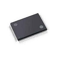
C8051F040-TB Silicon Laboratories Inc, C8051F040-TB Datasheet - Page 105

C8051F040-TB
Manufacturer Part Number
C8051F040-TB
Description
BOARD PROTOTYPING W/C8051F040
Manufacturer
Silicon Laboratories Inc
Type
MCUr
Specifications of C8051F040-TB
Contents
Board
Processor To Be Evaluated
C8051F04x
Interface Type
USB
Lead Free Status / RoHS Status
Contains lead / RoHS non-compliant
For Use With/related Products
C8051F040
Lead Free Status / Rohs Status
Lead free / RoHS Compliant
- Current page: 105 of 328
- Download datasheet (3Mb)
8.
Each C8051F040/1/2/3 devices include two on-chip 12-bit voltage-mode Digital-to-Analog Converters
(DACs). Each DAC has an output swing of 0 V to (VREF – 1 LSB) for a corresponding input code range of
0x000 to 0xFFF. The DACs may be enabled/disabled via their corresponding control registers, DAC0CN
and DAC1CN. While disabled, the DAC output is maintained in a high-impedance state, and the DAC sup-
ply current falls to 1 µA or less. The voltage reference for each DAC is supplied at the VREFD pin
(C8051F040/2 devices) or the VREF pin (C8051F041/3 devices). Note that the VREF pin on C8051F041/3
devices may be driven by the internal voltage reference or an external source. If the internal voltage refer-
ence is used it must be enabled in order for the DAC outputs to be valid. See
ence (C8051F040/2/4/6)” on page 113
page 117
DACs, 12-Bit Voltage Mode (C8051F040/1/2/3 Only)
for more information on configuring the voltage reference for the DACs.
DAC0MD1
DAC0MD0
DAC1MD1
DAC1MD0
DAC0DF2
DAC0DF1
DAC0DF0
DAC1DF2
DAC1DF1
DAC1DF0
DAC0EN
DAC1EN
Figure 8.1. DAC Functional Block Diagram
8
8
8
8
8
8
8
8
or
Section “10. Voltage Reference (C8051F041/3/5/7)” on
12
12
Rev. 1.5
REF
REF
DAC0
DAC1
C8051F040/1/2/3/4/5/6/7
AGND
AGND
Section “9. Voltage Refer-
AV+
AV+
DAC0
DAC1
105
Related parts for C8051F040-TB
Image
Part Number
Description
Manufacturer
Datasheet
Request
R
Part Number:
Description:
SMD/C°/SINGLE-ENDED OUTPUT SILICON OSCILLATOR
Manufacturer:
Silicon Laboratories Inc
Part Number:
Description:
Manufacturer:
Silicon Laboratories Inc
Datasheet:
Part Number:
Description:
N/A N/A/SI4010 AES KEYFOB DEMO WITH LCD RX
Manufacturer:
Silicon Laboratories Inc
Datasheet:
Part Number:
Description:
N/A N/A/SI4010 SIMPLIFIED KEY FOB DEMO WITH LED RX
Manufacturer:
Silicon Laboratories Inc
Datasheet:
Part Number:
Description:
N/A/-40 TO 85 OC/EZLINK MODULE; F930/4432 HIGH BAND (REV E/B1)
Manufacturer:
Silicon Laboratories Inc
Part Number:
Description:
EZLink Module; F930/4432 Low Band (rev e/B1)
Manufacturer:
Silicon Laboratories Inc
Part Number:
Description:
I°/4460 10 DBM RADIO TEST CARD 434 MHZ
Manufacturer:
Silicon Laboratories Inc
Part Number:
Description:
I°/4461 14 DBM RADIO TEST CARD 868 MHZ
Manufacturer:
Silicon Laboratories Inc
Part Number:
Description:
I°/4463 20 DBM RFSWITCH RADIO TEST CARD 460 MHZ
Manufacturer:
Silicon Laboratories Inc
Part Number:
Description:
I°/4463 20 DBM RADIO TEST CARD 868 MHZ
Manufacturer:
Silicon Laboratories Inc
Part Number:
Description:
I°/4463 27 DBM RADIO TEST CARD 868 MHZ
Manufacturer:
Silicon Laboratories Inc
Part Number:
Description:
I°/4463 SKYWORKS 30 DBM RADIO TEST CARD 915 MHZ
Manufacturer:
Silicon Laboratories Inc
Part Number:
Description:
N/A N/A/-40 TO 85 OC/4463 RFMD 30 DBM RADIO TEST CARD 915 MHZ
Manufacturer:
Silicon Laboratories Inc
Part Number:
Description:
I°/4463 20 DBM RADIO TEST CARD 169 MHZ
Manufacturer:
Silicon Laboratories Inc


