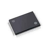
C8051F040-TB Silicon Laboratories Inc, C8051F040-TB Datasheet - Page 311

C8051F040-TB
Manufacturer Part Number
C8051F040-TB
Description
BOARD PROTOTYPING W/C8051F040
Manufacturer
Silicon Laboratories Inc
Type
MCUr
Specifications of C8051F040-TB
Contents
Board
Processor To Be Evaluated
C8051F04x
Interface Type
USB
Lead Free Status / RoHS Status
Contains lead / RoHS non-compliant
For Use With/related Products
C8051F040
Lead Free Status / Rohs Status
Lead free / RoHS Compliant
- Current page: 311 of 328
- Download datasheet (3Mb)
24.2.4. Frequency Output Mode
Frequency Output Mode produces a programmable-frequency square wave on the module’s associated
CEXn pin. The capture/compare module high byte holds the number of PCA clocks to count before the out-
put is toggled. The frequency of the square wave is then defined by Equation 24.1, where F
quency of the clock selected by the CPS2-0 bits in the PCA mode register, PCA0MD.
Note: A value of 0x00 in the PCA0CPHn register is equal to 256 for this equation.
The lower byte of the capture/compare module is compared to the PCA0 counter low byte; on a match,
CEXn is toggled and the offset held in the high byte is added to the matched value in PCA0CPLn. Fre-
quency Output Mode is enabled by setting the ECOMn, TOGn, and PWMn bits in the PCA0CPMn register.
W
P
M
1
6
n
0
PCA0CPMn
E
C
O
M
n
C
A
P
P
n
0 0 0
C
A
P
N
n
M
A
T
n
O
G
T
n
1
W
M
P
n
E
C
C
F
n
0
PCA Timebase
Equation 24.1. Square Wave Frequency Output
Enable
Figure 24.7. PCA Frequency Output Mode
Comparator
PCA0CPLn
PCA0L
8-bit
F
sqr
=
---------------------------------------- -
2 PCA0CPHn
Rev. 1.5
match
Enable
Adder
8-bit Adder
F
C8051F040/1/2/3/4/5/6/7
PCA
Toggle
TOGn
0
1
CEXn
PCA0CPHn
Crossbar
PCA
Port I/O
is the fre-
309
Related parts for C8051F040-TB
Image
Part Number
Description
Manufacturer
Datasheet
Request
R
Part Number:
Description:
SMD/C°/SINGLE-ENDED OUTPUT SILICON OSCILLATOR
Manufacturer:
Silicon Laboratories Inc
Part Number:
Description:
Manufacturer:
Silicon Laboratories Inc
Datasheet:
Part Number:
Description:
N/A N/A/SI4010 AES KEYFOB DEMO WITH LCD RX
Manufacturer:
Silicon Laboratories Inc
Datasheet:
Part Number:
Description:
N/A N/A/SI4010 SIMPLIFIED KEY FOB DEMO WITH LED RX
Manufacturer:
Silicon Laboratories Inc
Datasheet:
Part Number:
Description:
N/A/-40 TO 85 OC/EZLINK MODULE; F930/4432 HIGH BAND (REV E/B1)
Manufacturer:
Silicon Laboratories Inc
Part Number:
Description:
EZLink Module; F930/4432 Low Band (rev e/B1)
Manufacturer:
Silicon Laboratories Inc
Part Number:
Description:
I°/4460 10 DBM RADIO TEST CARD 434 MHZ
Manufacturer:
Silicon Laboratories Inc
Part Number:
Description:
I°/4461 14 DBM RADIO TEST CARD 868 MHZ
Manufacturer:
Silicon Laboratories Inc
Part Number:
Description:
I°/4463 20 DBM RFSWITCH RADIO TEST CARD 460 MHZ
Manufacturer:
Silicon Laboratories Inc
Part Number:
Description:
I°/4463 20 DBM RADIO TEST CARD 868 MHZ
Manufacturer:
Silicon Laboratories Inc
Part Number:
Description:
I°/4463 27 DBM RADIO TEST CARD 868 MHZ
Manufacturer:
Silicon Laboratories Inc
Part Number:
Description:
I°/4463 SKYWORKS 30 DBM RADIO TEST CARD 915 MHZ
Manufacturer:
Silicon Laboratories Inc
Part Number:
Description:
N/A N/A/-40 TO 85 OC/4463 RFMD 30 DBM RADIO TEST CARD 915 MHZ
Manufacturer:
Silicon Laboratories Inc
Part Number:
Description:
I°/4463 20 DBM RADIO TEST CARD 169 MHZ
Manufacturer:
Silicon Laboratories Inc


