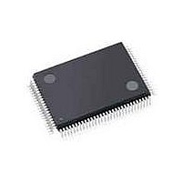
C8051F040-TB Silicon Laboratories Inc, C8051F040-TB Datasheet - Page 34

C8051F040-TB
Manufacturer Part Number
C8051F040-TB
Description
BOARD PROTOTYPING W/C8051F040
Manufacturer
Silicon Laboratories Inc
Type
MCUr
Specifications of C8051F040-TB
Contents
Board
Processor To Be Evaluated
C8051F04x
Interface Type
USB
Lead Free Status / RoHS Status
Contains lead / RoHS non-compliant
For Use With/related Products
C8051F040
Lead Free Status / Rohs Status
Lead free / RoHS Compliant
- Current page: 34 of 328
- Download datasheet (3Mb)
C8051F040/1/2/3/4/5/6/7
1.10. Comparators and DACs
Each C8051F040/1/2/3 MCU has two 12-bit DACs, and all C8051F04x devices have three comparators on
chip. The MCU data and control interface to each comparator and DAC is via the Special Function Regis-
ters. The MCU can place any DAC or comparator in low power shutdown mode.
The comparators have software programmable hysteresis and response time. Each comparator can gen-
erate an interrupt on its rising edge, falling edge, or both; these interrupts are capable of waking up the
MCU from sleep mode. The comparators' output state can also be polled in software. The comparator out-
puts can be programmed to appear on the Port I/O pins via the Crossbar.
The DACs are voltage output mode and include a flexible output scheduling mechanism. This scheduling
mechanism allows DAC output updates to be forced by a software write or a Timer 2, 3, or 4 overflow. The
DAC voltage reference is supplied via the dedicated VREFD input pin on C8051F040/2 devices or via the
internal voltage reference on C8051F041/3 devices. The DACs are especially useful as references for the
comparators or offsets for the differential inputs of the ADC.
34
(C 8051F040/1/2/3 only)
(C 8051F040/1/2/3 only)
(Port I/O )
DAC0
DAC1
CPn+
CPn-
C om parator inputs
Port 2.[7:2]
Figure 1.14. Comparator and DAC Diagram
CPn O utput
+
-
CPn
3 Com parators
VREF
DAC 0
VREF
DAC 1
CRO SSBAR
Rev. 1.5
SFR's
(Data
Cntrl)
and
Interrupt
H andler
C IP-51
and
Related parts for C8051F040-TB
Image
Part Number
Description
Manufacturer
Datasheet
Request
R
Part Number:
Description:
SMD/C°/SINGLE-ENDED OUTPUT SILICON OSCILLATOR
Manufacturer:
Silicon Laboratories Inc
Part Number:
Description:
Manufacturer:
Silicon Laboratories Inc
Datasheet:
Part Number:
Description:
N/A N/A/SI4010 AES KEYFOB DEMO WITH LCD RX
Manufacturer:
Silicon Laboratories Inc
Datasheet:
Part Number:
Description:
N/A N/A/SI4010 SIMPLIFIED KEY FOB DEMO WITH LED RX
Manufacturer:
Silicon Laboratories Inc
Datasheet:
Part Number:
Description:
N/A/-40 TO 85 OC/EZLINK MODULE; F930/4432 HIGH BAND (REV E/B1)
Manufacturer:
Silicon Laboratories Inc
Part Number:
Description:
EZLink Module; F930/4432 Low Band (rev e/B1)
Manufacturer:
Silicon Laboratories Inc
Part Number:
Description:
I°/4460 10 DBM RADIO TEST CARD 434 MHZ
Manufacturer:
Silicon Laboratories Inc
Part Number:
Description:
I°/4461 14 DBM RADIO TEST CARD 868 MHZ
Manufacturer:
Silicon Laboratories Inc
Part Number:
Description:
I°/4463 20 DBM RFSWITCH RADIO TEST CARD 460 MHZ
Manufacturer:
Silicon Laboratories Inc
Part Number:
Description:
I°/4463 20 DBM RADIO TEST CARD 868 MHZ
Manufacturer:
Silicon Laboratories Inc
Part Number:
Description:
I°/4463 27 DBM RADIO TEST CARD 868 MHZ
Manufacturer:
Silicon Laboratories Inc
Part Number:
Description:
I°/4463 SKYWORKS 30 DBM RADIO TEST CARD 915 MHZ
Manufacturer:
Silicon Laboratories Inc
Part Number:
Description:
N/A N/A/-40 TO 85 OC/4463 RFMD 30 DBM RADIO TEST CARD 915 MHZ
Manufacturer:
Silicon Laboratories Inc
Part Number:
Description:
I°/4463 20 DBM RADIO TEST CARD 169 MHZ
Manufacturer:
Silicon Laboratories Inc


