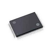
C8051F040-TB Silicon Laboratories Inc, C8051F040-TB Datasheet - Page 184

C8051F040-TB
Manufacturer Part Number
C8051F040-TB
Description
BOARD PROTOTYPING W/C8051F040
Manufacturer
Silicon Laboratories Inc
Type
MCUr
Specifications of C8051F040-TB
Contents
Board
Processor To Be Evaluated
C8051F04x
Interface Type
USB
Lead Free Status / RoHS Status
Contains lead / RoHS non-compliant
For Use With/related Products
C8051F040
Lead Free Status / Rohs Status
Lead free / RoHS Compliant
- Current page: 184 of 328
- Download datasheet (3Mb)
C8051F040/1/2/3/4/5/6/7
184
Bits 7-0: FLACL: Flash Access Limit.
Bit7:
Bit6:
Bits5-1:
Bit0:
FOSE
R/W
R/W
Bit7
Bit7
This register holds the high byte of the 16-bit program memory read/write/erase limit
address. The entire 16-bit access limit address value is calculated as 0xNN00 where NN is
replaced by contents of FLACL. A write to this register sets the Flash Access Limit. This reg-
ister can only be written once after any reset. Any subsequent writes are ignored until the
next reset.
FOSE: Flash One-Shot Timer Enable
This is the timer that turns off the sense amps after a Flash read.
0: Flash One-Shot Timer disabled.
1: Flash One-Shot Timer enabled (recommended setting).
FRAE: Flash Read Always Enable
0: Flash reads occur as necessary (recommended setting).
1: Flash reads occur every system clock cycle.
RESERVED. Read = 00000b. Must Write 00000b.
FLWE: Flash Write/Erase Enable
This bit must be set to allow Flash writes/erases from user software.
0: Flash writes/erases disabled.
1: Flash writes/erases enabled.
FRAE
R/W
Bit6
R/W
Bit6
SFR Definition 15.2. FLSCL: Flash Memory Control
SFR Definition 15.1. FLACL: Flash Access Limit
Reserved Reserved Reserved Reserved Reserved
R/W
Bit5
R/W
Bit5
R/W
Bit4
R/W
Bit4
Rev. 1.5
R/W
Bit3
R/W
Bit3
R/W
Bit2
R/W
Bit2
R/W
Bit1
R/W
Bit1
SFR Address:
SFR Address:
SFR Page:
SFR Page:
FLWE
R/W
Bit0
R/W
Bit0
0xB7
F
SFR Address:
00000000
SFR Address:
0xB7
0
Reset Value
10000000
Reset Value
Related parts for C8051F040-TB
Image
Part Number
Description
Manufacturer
Datasheet
Request
R
Part Number:
Description:
SMD/C°/SINGLE-ENDED OUTPUT SILICON OSCILLATOR
Manufacturer:
Silicon Laboratories Inc
Part Number:
Description:
Manufacturer:
Silicon Laboratories Inc
Datasheet:
Part Number:
Description:
N/A N/A/SI4010 AES KEYFOB DEMO WITH LCD RX
Manufacturer:
Silicon Laboratories Inc
Datasheet:
Part Number:
Description:
N/A N/A/SI4010 SIMPLIFIED KEY FOB DEMO WITH LED RX
Manufacturer:
Silicon Laboratories Inc
Datasheet:
Part Number:
Description:
N/A/-40 TO 85 OC/EZLINK MODULE; F930/4432 HIGH BAND (REV E/B1)
Manufacturer:
Silicon Laboratories Inc
Part Number:
Description:
EZLink Module; F930/4432 Low Band (rev e/B1)
Manufacturer:
Silicon Laboratories Inc
Part Number:
Description:
I°/4460 10 DBM RADIO TEST CARD 434 MHZ
Manufacturer:
Silicon Laboratories Inc
Part Number:
Description:
I°/4461 14 DBM RADIO TEST CARD 868 MHZ
Manufacturer:
Silicon Laboratories Inc
Part Number:
Description:
I°/4463 20 DBM RFSWITCH RADIO TEST CARD 460 MHZ
Manufacturer:
Silicon Laboratories Inc
Part Number:
Description:
I°/4463 20 DBM RADIO TEST CARD 868 MHZ
Manufacturer:
Silicon Laboratories Inc
Part Number:
Description:
I°/4463 27 DBM RADIO TEST CARD 868 MHZ
Manufacturer:
Silicon Laboratories Inc
Part Number:
Description:
I°/4463 SKYWORKS 30 DBM RADIO TEST CARD 915 MHZ
Manufacturer:
Silicon Laboratories Inc
Part Number:
Description:
N/A N/A/-40 TO 85 OC/4463 RFMD 30 DBM RADIO TEST CARD 915 MHZ
Manufacturer:
Silicon Laboratories Inc
Part Number:
Description:
I°/4463 20 DBM RADIO TEST CARD 169 MHZ
Manufacturer:
Silicon Laboratories Inc


