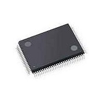
C8051F040-TB Silicon Laboratories Inc, C8051F040-TB Datasheet - Page 240

C8051F040-TB
Manufacturer Part Number
C8051F040-TB
Description
BOARD PROTOTYPING W/C8051F040
Manufacturer
Silicon Laboratories Inc
Type
MCUr
Specifications of C8051F040-TB
Contents
Board
Processor To Be Evaluated
C8051F04x
Interface Type
USB
Lead Free Status / RoHS Status
Contains lead / RoHS non-compliant
For Use With/related Products
C8051F040
Lead Free Status / Rohs Status
Lead free / RoHS Compliant
- Current page: 240 of 328
- Download datasheet (3Mb)
C8051F040/1/2/3/4/5/6/7
Figure 19.2 shows a typical SMBus configuration. The SMBus0 interface will work at any voltage between
3.0 V and 5.0 V and different devices on the bus may operate at different voltage levels. The bi-directional
SCL (serial clock) and SDA (serial data) lines must be connected to a positive power supply voltage
through a pullup resistor or similar circuit. Every device connected to the bus must have an open-drain or
open-collector output for both the SCL and SDA lines, so that both are pulled high when the bus is free.
The maximum number of devices on the bus is limited only by the requirement that the rise and fall times
on the bus will not exceed 300 ns and 1000 ns, respectively.
19.1. Supporting Documents
It is assumed the reader is familiar with or has access to the following supporting documents:
•
•
240
I
System Management Bus Specification -- Version 1.1, SBS Implementers Forum.
2
C Manual (AN10216-01) -- March 24, 2003, Philips Semiconductor.
V
DD
= 5 V
Figure 19.2. Typical SMBus Configuration
V
Master
Device
DD
= 3 V
Rev. 1.5
Device 1
V
Slave
DD
= 5 V
Device 2
V
Slave
DD
= 3 V
SDA
SCL
Related parts for C8051F040-TB
Image
Part Number
Description
Manufacturer
Datasheet
Request
R
Part Number:
Description:
SMD/C°/SINGLE-ENDED OUTPUT SILICON OSCILLATOR
Manufacturer:
Silicon Laboratories Inc
Part Number:
Description:
Manufacturer:
Silicon Laboratories Inc
Datasheet:
Part Number:
Description:
N/A N/A/SI4010 AES KEYFOB DEMO WITH LCD RX
Manufacturer:
Silicon Laboratories Inc
Datasheet:
Part Number:
Description:
N/A N/A/SI4010 SIMPLIFIED KEY FOB DEMO WITH LED RX
Manufacturer:
Silicon Laboratories Inc
Datasheet:
Part Number:
Description:
N/A/-40 TO 85 OC/EZLINK MODULE; F930/4432 HIGH BAND (REV E/B1)
Manufacturer:
Silicon Laboratories Inc
Part Number:
Description:
EZLink Module; F930/4432 Low Band (rev e/B1)
Manufacturer:
Silicon Laboratories Inc
Part Number:
Description:
I°/4460 10 DBM RADIO TEST CARD 434 MHZ
Manufacturer:
Silicon Laboratories Inc
Part Number:
Description:
I°/4461 14 DBM RADIO TEST CARD 868 MHZ
Manufacturer:
Silicon Laboratories Inc
Part Number:
Description:
I°/4463 20 DBM RFSWITCH RADIO TEST CARD 460 MHZ
Manufacturer:
Silicon Laboratories Inc
Part Number:
Description:
I°/4463 20 DBM RADIO TEST CARD 868 MHZ
Manufacturer:
Silicon Laboratories Inc
Part Number:
Description:
I°/4463 27 DBM RADIO TEST CARD 868 MHZ
Manufacturer:
Silicon Laboratories Inc
Part Number:
Description:
I°/4463 SKYWORKS 30 DBM RADIO TEST CARD 915 MHZ
Manufacturer:
Silicon Laboratories Inc
Part Number:
Description:
N/A N/A/-40 TO 85 OC/4463 RFMD 30 DBM RADIO TEST CARD 915 MHZ
Manufacturer:
Silicon Laboratories Inc
Part Number:
Description:
I°/4463 20 DBM RADIO TEST CARD 169 MHZ
Manufacturer:
Silicon Laboratories Inc


