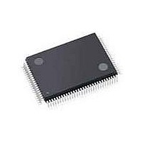
C8051F040-TB Silicon Laboratories Inc, C8051F040-TB Datasheet - Page 36

C8051F040-TB
Manufacturer Part Number
C8051F040-TB
Description
BOARD PROTOTYPING W/C8051F040
Manufacturer
Silicon Laboratories Inc
Type
MCUr
Specifications of C8051F040-TB
Contents
Board
Processor To Be Evaluated
C8051F04x
Interface Type
USB
Lead Free Status / RoHS Status
Contains lead / RoHS non-compliant
For Use With/related Products
C8051F040
Lead Free Status / Rohs Status
Lead free / RoHS Compliant
- Current page: 36 of 328
- Download datasheet (3Mb)
C8051F040/1/2/3/4/5/6/7
3.
Table 3.1. Global DC Electrical Characteristics
–40 to +85 °C, 25 MHz System Clock unless otherwise specified.
36
Analog Supply Voltage
Analog Supply Current
Analog Supply Current with
analog sub-systems inactive
Analog-to-Digital Supply
Delta (|V
Digital Supply Voltage
Digital Supply Current with
CPU active
(Normal Mode)
Digital Supply Current with
CPU inactive (not accessing
Flash) (Idle Mode)
Digital Supply Current
(shutdown) (Stop Mode)
Digital Supply RAM Data
Retention Voltage
Specified Operating
Temperature Range
SYSCLK (system clock
frequency)
Tsysl (SYSCLK low time)
Tsysh (SYSCLK high time)
Notes:
1. Analog Supply AV+ must be greater than 1 V for
2. SYSCLK must be at least 32 kHz to enable debugging.
Global DC Electrical Characteristic
DD
Parameter
2
- AV+|)
1
Internal REF, ADC, DAC, Com-
parators all active
Internal REF, ADC, DAC, Com-
parators all disabled, oscillator
disabled
V
V
V
V
V
V
Oscillator not running
DD
DD
DD
DD
DD
DD
= 2.7 V, Clock = 25 MHz
= 2.7 V, Clock = 1 MHz
= 2.7 V, Clock = 32 kHz
= 2.7 V, Clock = 25 MHz
= 2.7 V, Clock = 1 MHz
= 2.7 V, Clock = 32 kHz
Conditions
Rev. 1.5
V
DD
monitor to operate.
Min
–40
2.7
2.7
18
18
—
—
—
—
—
—
—
—
—
—
—
0
Typ
3.0
1.7
0.2
3.0
0.5
0.2
0.2
1.5
10
20
10
—
—
—
—
—
5
Max
+85
3.6
0.5
3.6
25
—
—
—
—
—
—
—
—
—
—
—
—
Units
MHz
mA
mA
mA
mA
mA
µA
µA
µA
µA
°C
ns
ns
V
V
V
V
Related parts for C8051F040-TB
Image
Part Number
Description
Manufacturer
Datasheet
Request
R
Part Number:
Description:
SMD/C°/SINGLE-ENDED OUTPUT SILICON OSCILLATOR
Manufacturer:
Silicon Laboratories Inc
Part Number:
Description:
Manufacturer:
Silicon Laboratories Inc
Datasheet:
Part Number:
Description:
N/A N/A/SI4010 AES KEYFOB DEMO WITH LCD RX
Manufacturer:
Silicon Laboratories Inc
Datasheet:
Part Number:
Description:
N/A N/A/SI4010 SIMPLIFIED KEY FOB DEMO WITH LED RX
Manufacturer:
Silicon Laboratories Inc
Datasheet:
Part Number:
Description:
N/A/-40 TO 85 OC/EZLINK MODULE; F930/4432 HIGH BAND (REV E/B1)
Manufacturer:
Silicon Laboratories Inc
Part Number:
Description:
EZLink Module; F930/4432 Low Band (rev e/B1)
Manufacturer:
Silicon Laboratories Inc
Part Number:
Description:
I°/4460 10 DBM RADIO TEST CARD 434 MHZ
Manufacturer:
Silicon Laboratories Inc
Part Number:
Description:
I°/4461 14 DBM RADIO TEST CARD 868 MHZ
Manufacturer:
Silicon Laboratories Inc
Part Number:
Description:
I°/4463 20 DBM RFSWITCH RADIO TEST CARD 460 MHZ
Manufacturer:
Silicon Laboratories Inc
Part Number:
Description:
I°/4463 20 DBM RADIO TEST CARD 868 MHZ
Manufacturer:
Silicon Laboratories Inc
Part Number:
Description:
I°/4463 27 DBM RADIO TEST CARD 868 MHZ
Manufacturer:
Silicon Laboratories Inc
Part Number:
Description:
I°/4463 SKYWORKS 30 DBM RADIO TEST CARD 915 MHZ
Manufacturer:
Silicon Laboratories Inc
Part Number:
Description:
N/A N/A/-40 TO 85 OC/4463 RFMD 30 DBM RADIO TEST CARD 915 MHZ
Manufacturer:
Silicon Laboratories Inc
Part Number:
Description:
I°/4463 20 DBM RADIO TEST CARD 169 MHZ
Manufacturer:
Silicon Laboratories Inc


