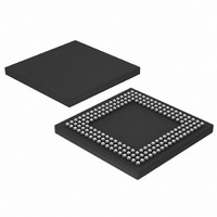
LPC3130FET180,551 NXP Semiconductors, LPC3130FET180,551 Datasheet - Page 21

LPC3130FET180,551
Manufacturer Part Number
LPC3130FET180,551
Description
IC ARM9 MCU 180MHZ 180-TFBGA
Manufacturer
NXP Semiconductors
Series
LPC3000r
Datasheet
1.OM11024.pdf
(72 pages)
Specifications of LPC3130FET180,551
Package / Case
180-TFBGA
Core Processor
ARM9
Core Size
32-Bit
Speed
180MHz
Connectivity
EBI/EMI, I²C, MMC, SPI, UART/USART, USB OTG
Peripherals
DMA, I²S, LCD, PWM, WDT
Program Memory Type
ROMless
Ram Size
96K x 8
Voltage - Supply (vcc/vdd)
1.1 V ~ 3.6 V
Data Converters
A/D 4x10b
Oscillator Type
External
Operating Temperature
-40°C ~ 85°C
Processor Series
LPC31
Core
ARM926EJ-S
Data Bus Width
16 bit, 32 bit
Data Ram Size
96 KB
Interface Type
I2C/I2S/UART/USB
Maximum Clock Frequency
180 MHz
Number Of Timers
4
Operating Supply Voltage
2.7 V to 3.6 V
Maximum Operating Temperature
+ 85 C
Mounting Style
SMD/SMT
3rd Party Development Tools
MDK-ARM, RL-ARM, ULINK2
Minimum Operating Temperature
- 40 C
On-chip Adc
4-ch x 10-bit
Cpu Family
LPC3000
Device Core
ARM926EJ-S
Device Core Size
16/32Bit
Frequency (max)
180MHz
Program Memory Size
Not Required
Total Internal Ram Size
96KB
Number Of Timers - General Purpose
4
Operating Supply Voltage (typ)
1.2/1.8/2.8/3.3/5V
Operating Supply Voltage (max)
1.3/3.6V
Operating Supply Voltage (min)
1/1.1/1.65/2.7V
Instruction Set Architecture
RISC
Operating Temp Range
-40C to 85C
Operating Temperature Classification
Industrial
Mounting
Surface Mount
Pin Count
180
Package Type
TFBGA
Package
180TFBGA
Family Name
LPC3000
Maximum Speed
180 MHz
Lead Free Status / RoHS Status
Lead free / RoHS Compliant
For Use With
568-4850 - KIT EVAL FOR LPC313X568-4062 - DEBUGGER J-LINK JTAG568-4061 - DEBUGGER U-LINK2 JTAG FOR NXP
Number Of I /o
-
Eeprom Size
-
Program Memory Size
-
Lead Free Status / Rohs Status
Lead free / RoHS Compliant
Other names
568-4696
935288013551
LPC3130FET180-S
935288013551
LPC3130FET180-S
Available stocks
Company
Part Number
Manufacturer
Quantity
Price
Company:
Part Number:
LPC3130FET180,551
Manufacturer:
NXP Semiconductors
Quantity:
10 000
NXP Semiconductors
LPC3130_3131
Preliminary data sheet
6.13 Multi-layer AHB
The following blocks can generate interrupts:
The multi-layer AHB is an interconnection scheme based on the AHB protocol that
enables parallel access paths between multiple masters and slaves in a system.
Multiple masters can have access to different slaves at the same time.
Figure 5
AHB masters and slaves are numbered according to their AHB port number.
•
•
•
•
•
•
•
•
•
•
•
•
•
•
•
•
•
Visibility of the interrupt’s request state before masking.
Support for nesting of interrupt service routines.
Interrupts routed to IRQ and to FIQ are vectored.
Level interrupt support.
NAND flash controller
USB 2.0 high-speed OTG
Event router
10-bit ADC
UART
LCD
MCI
SPI
I2C0 and I2C1 controllers
Timer0, Timer1, Timer2, and Timer3
I
I
DMA
2
2
S transmit: I2STX_0 and I2STX_1
S receive: I2SRX_0 and I2SRX_1
gives an overview of the multi-layer AHB configuration in the LPC3130/3131.
All information provided in this document is subject to legal disclaimers.
Rev. 1.04 — 27 May 2010
Low-cost, low-power ARM926EJ-S microcontrollers
LPC3130/3131
© NXP B.V. 2010. All rights reserved.
21 of 72


