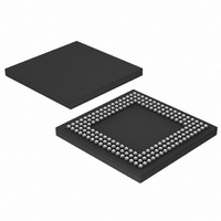
LPC3130FET180,551 NXP Semiconductors, LPC3130FET180,551 Datasheet - Page 25

LPC3130FET180,551
Manufacturer Part Number
LPC3130FET180,551
Description
IC ARM9 MCU 180MHZ 180-TFBGA
Manufacturer
NXP Semiconductors
Series
LPC3000r
Datasheet
1.OM11024.pdf
(72 pages)
Specifications of LPC3130FET180,551
Package / Case
180-TFBGA
Core Processor
ARM9
Core Size
32-Bit
Speed
180MHz
Connectivity
EBI/EMI, I²C, MMC, SPI, UART/USART, USB OTG
Peripherals
DMA, I²S, LCD, PWM, WDT
Program Memory Type
ROMless
Ram Size
96K x 8
Voltage - Supply (vcc/vdd)
1.1 V ~ 3.6 V
Data Converters
A/D 4x10b
Oscillator Type
External
Operating Temperature
-40°C ~ 85°C
Processor Series
LPC31
Core
ARM926EJ-S
Data Bus Width
16 bit, 32 bit
Data Ram Size
96 KB
Interface Type
I2C/I2S/UART/USB
Maximum Clock Frequency
180 MHz
Number Of Timers
4
Operating Supply Voltage
2.7 V to 3.6 V
Maximum Operating Temperature
+ 85 C
Mounting Style
SMD/SMT
3rd Party Development Tools
MDK-ARM, RL-ARM, ULINK2
Minimum Operating Temperature
- 40 C
On-chip Adc
4-ch x 10-bit
Cpu Family
LPC3000
Device Core
ARM926EJ-S
Device Core Size
16/32Bit
Frequency (max)
180MHz
Program Memory Size
Not Required
Total Internal Ram Size
96KB
Number Of Timers - General Purpose
4
Operating Supply Voltage (typ)
1.2/1.8/2.8/3.3/5V
Operating Supply Voltage (max)
1.3/3.6V
Operating Supply Voltage (min)
1/1.1/1.65/2.7V
Instruction Set Architecture
RISC
Operating Temp Range
-40C to 85C
Operating Temperature Classification
Industrial
Mounting
Surface Mount
Pin Count
180
Package Type
TFBGA
Package
180TFBGA
Family Name
LPC3000
Maximum Speed
180 MHz
Lead Free Status / RoHS Status
Lead free / RoHS Compliant
For Use With
568-4850 - KIT EVAL FOR LPC313X568-4062 - DEBUGGER J-LINK JTAG568-4061 - DEBUGGER U-LINK2 JTAG FOR NXP
Number Of I /o
-
Eeprom Size
-
Program Memory Size
-
Lead Free Status / Rohs Status
Lead free / RoHS Compliant
Other names
568-4696
935288013551
LPC3130FET180-S
935288013551
LPC3130FET180-S
Available stocks
Company
Part Number
Manufacturer
Quantity
Price
Company:
Part Number:
LPC3130FET180,551
Manufacturer:
NXP Semiconductors
Quantity:
10 000
NXP Semiconductors
LPC3130_3131
Preliminary data sheet
Fig 6. CGU block diagram
EXTERNAL
CRYSTAL
I2SRX_BCK1
I2SRX_BCK0
I2SRX_WS0
I2SRX_WS1
The LPC3130/3131 has 11 clock domains (n = 11). The number of fractional dividers m depends on the clock domain.
clock resources
6.16 Watchdog Timer (WDT)
OSCILLATOR
The watchdog timer can be used to generate a system reset if there is a CPU/software
crash. In addition, the watchdog timer can be used as an ordinary timer.
how the watchdog timer module is connected in the system.
This module has the following features:
•
•
•
•
•
Based on the input of the Watchdog timer (see also
generate a system-wide reset in the case of a system stall.
In the event of a software or hardware failure, generates a chip-wide reset request
when its programmed time-out period has expired (output m1).
Watchdog counter can be reset by a periodical software trigger.
After a reset, a register will indicate whether a reset has occurred because of a
watchdog generated reset.
Watchdog timer can also be used as a normal timer (output m0).
All information provided in this document is subject to legal disclaimers.
Rev. 1.04 — 27 May 2010
I
2
SYSTEM
S/AUDIO
PLL
PLL
Low-cost, low-power ARM926EJ-S microcontrollers
SWITCHBOX
CLOCK DOMAIN 0
CLOCK DOMAIN n
BASE
subdomain clocks
Section
FRACTIONAL
FRACTIONAL
DIVIDER m
LPC3130/3131
DIVIDER 0
6.16), the CGU can
© NXP B.V. 2010. All rights reserved.
Figure 7
clock outputs
002aae085
to modules
shows
25 of 72


