COP8SGR728M7/NOPB National Semiconductor, COP8SGR728M7/NOPB Datasheet - Page 19
COP8SGR728M7/NOPB
Manufacturer Part Number
COP8SGR728M7/NOPB
Description
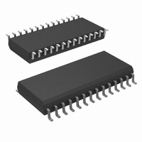
MCU 8BIT CMOS ROM OTP 28-SOIC
Manufacturer
National Semiconductor
Series
COP8™ 8SGr
Datasheet
1.COP8SGE728N8NOPB.pdf
(62 pages)
Specifications of COP8SGR728M7/NOPB
Core Processor
COP8
Core Size
8-Bit
Speed
15MHz
Connectivity
Microwire/Plus (SPI), UART/USART
Peripherals
POR, PWM, WDT
Number Of I /o
24
Program Memory Size
32KB (32K x 8)
Program Memory Type
OTP
Ram Size
512 x 8
Voltage - Supply (vcc/vdd)
2.7 V ~ 5.5 V
Oscillator Type
Internal
Operating Temperature
-40°C ~ 125°C
Package / Case
28-SOIC
Data Bus Width
8 bit
Maximum Clock Frequency
15 MHz
Data Ram Size
512 B
Number Of Programmable I/os
40
Number Of Timers
3
Height
2.34 mm
Interface Type
USART
Length
17.91 mm
Maximum Operating Temperature
+ 125 C
Minimum Operating Temperature
- 40 C
Supply Voltage (max)
5.5 V
Supply Voltage (min)
2.7 V
Width
7.49 mm
For Use With
COP8SG-EPU - BOARD PROTOTYPE/TARGET COP8
Lead Free Status / RoHS Status
Lead free / RoHS Compliant
Eeprom Size
-
Data Converters
-
Lead Free Status / Rohs Status
Details
Other names
COP8SGR728M7


5.0 Functional Description
DOG logic and the Clock Monitor detector armed, with the
WATCHDOG service window bits set and the Clock Monitor
bit set. The WATCHDOG and Clock Monitor circuits are
inhibited during reset. The WATCHDOG service window bits
being initialized high default to the maximum WATCHDOG
service window of 64k t
being initialized high will cause a Clock Monitor error follow-
ing reset if the clock has not reached the minimum specified
frequency at the termination of reset. A Clock Monitor error
will cause an active low error output on pin G1. This error
output will continue until 16 t
the clock frequency reaching the minimum specified value,
at which time the G1 output will go high.
5.9.1 External Reset
The RESET input when pulled low initializes the device. The
RESET pin must be held low for a minimum of one instruc-
tion cycle to guarantee a valid reset. During Power-Up ini-
tialization, the user must ensure that the RESET pin is held
low until the device is within the specified V
R/C circuit on the RESET pin with a delay 5 times (5x)
greater than the power supply rise time or 15 µs whichever is
greater, is recommended. Reset should also be wide enough
to ensure crystal start-up upon Power-Up.
RESET may also be used to cause an exit from the HALT
mode.
A recommended reset circuit for this device is shown in
Figure 9 .
RC
5.9.2 On-Chip Power-On Reset
The on-chip reset circuit is selected by a bit in the ECON
register. When enabled, the device generates an internal
reset as V
reset circuitry is able to detect both fast and slow rise times
on V
antee an on-chip power-on-reset, V
less than the start voltage specified in the DC characteris-
tics. Also, if V
powering back up to the operating range. If this is not pos-
sible, it is recommended that external reset be used.
Under no circumstances should the RESET pin be allowed
to float. If the on-chip Power-On Reset feature is being used,
>
The device comes out of reset with both the WATCH-
5x power supply rise time or 15 µs, whichever is greater.
CC
FIGURE 9. Reset Circuit Using External Reset
(V
CC
CC
rises to a voltage level above 2.0V. The on-chip
rise time between 10 ns and 50 ms).To guar-
CC
be lowered to the start voltage before
C
clock cycles. The Clock Monitor bit
C
–32 t
CC
C
must start at a voltage
clock cycles following
10131714
CC
(Continued)
voltage. An
19
RESET pin should be connected directly, or through a
pull-up resistor, to V
detector will always preset the Idle timer to 0FFF(4096 t
At this time, the internal reset will be generated.
If the Power-On Reset feature is enabled, the internal reset
will not be turned off until the Idle timer underflows. The
internal reset will perform the same functions as external
reset. The user is responsible for ensuring that V
minimum level for the operating frequency within the 4096
t
additional internal resets occur as long as V
above 2.0V.
The contents of data registers and RAM are unknown fol-
lowing the on-chip reset.
C
FIGURE 10. Reset Timing (Power-On Reset Enabled)
. After the underflow, the logic is designed such that no
FIGURE 11. Reset Circuit Using Power-On Reset
with V
CC
. The output of the power-on reset
CC
Tied to RESET
10131716
CC
www.national.com
CC
10131715
is at the
remains
C
).
Related parts for COP8SGR728M7/NOPB
Image
Part Number
Description
Manufacturer
Datasheet
Request
R

Part Number:
Description:
National Semiconductor [8-Bit D/A Converter]
Manufacturer:
National Semiconductor
Datasheet:
Part Number:
Description:
National Semiconductor [Media Coprocessor]
Manufacturer:
National Semiconductor
Datasheet:
Part Number:
Description:
Digitally Controlled Tone and Volume Circuit with Stereo Audio Power Amplifier, Microphone Preamp Stage and National 3D Sound
Manufacturer:
National Semiconductor
Datasheet:
Part Number:
Description:
Digitally Controlled Tone and Volume Circuit with Stereo Audio Power Amplifier, Microphone Preamp Stage and National 3D Sound
Manufacturer:
National Semiconductor
Datasheet:
Part Number:
Description:
AC97 Rev 2 Codec with Sample Rate Conversion and National 3D Sound
Manufacturer:
National Semiconductor
Part Number:
Description:
Manufacturer:
National Semiconductor
Datasheet:
Part Number:
Description:
Manufacturer:
National Semiconductor
Datasheet:
Part Number:
Description:
General Purpose, Low Voltage, Low Power, Rail-to-Rail Output Operational Amplifiers
Manufacturer:
National Semiconductor
Datasheet:
Part Number:
Description:
8-bit 20 MSPS flash A/D converter.
Manufacturer:
National Semiconductor
Datasheet:
Part Number:
Description:
Low Noise Quad Operational Amplifier
Manufacturer:
National Semiconductor
Datasheet:
Part Number:
Description:
Quad Differential Line Receivers
Manufacturer:
National Semiconductor
Datasheet:
Part Number:
Description:
Quad High Speed Trapezoidal? Bus Transceiver
Manufacturer:
National Semiconductor
Datasheet:
Part Number:
Description:
Dual Line Receiver
Manufacturer:
National Semiconductor
Datasheet:
Part Number:
Description:
TTL to 10k ECL Level Translator with Latch
Manufacturer:
National Semiconductor
Datasheet: