COP8SGR728M7/NOPB National Semiconductor, COP8SGR728M7/NOPB Datasheet - Page 7
COP8SGR728M7/NOPB
Manufacturer Part Number
COP8SGR728M7/NOPB
Description
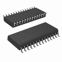
MCU 8BIT CMOS ROM OTP 28-SOIC
Manufacturer
National Semiconductor
Series
COP8™ 8SGr
Datasheet
1.COP8SGE728N8NOPB.pdf
(62 pages)
Specifications of COP8SGR728M7/NOPB
Core Processor
COP8
Core Size
8-Bit
Speed
15MHz
Connectivity
Microwire/Plus (SPI), UART/USART
Peripherals
POR, PWM, WDT
Number Of I /o
24
Program Memory Size
32KB (32K x 8)
Program Memory Type
OTP
Ram Size
512 x 8
Voltage - Supply (vcc/vdd)
2.7 V ~ 5.5 V
Oscillator Type
Internal
Operating Temperature
-40°C ~ 125°C
Package / Case
28-SOIC
Data Bus Width
8 bit
Maximum Clock Frequency
15 MHz
Data Ram Size
512 B
Number Of Programmable I/os
40
Number Of Timers
3
Height
2.34 mm
Interface Type
USART
Length
17.91 mm
Maximum Operating Temperature
+ 125 C
Minimum Operating Temperature
- 40 C
Supply Voltage (max)
5.5 V
Supply Voltage (min)
2.7 V
Width
7.49 mm
For Use With
COP8SG-EPU - BOARD PROTOTYPE/TARGET COP8
Lead Free Status / RoHS Status
Lead free / RoHS Compliant
Eeprom Size
-
Data Converters
-
Lead Free Status / Rohs Status
Details
Other names
COP8SGR728M7


Operating Voltage
Power Supply Rise Time
V
Power Supply Ripple (Note 4)
Supply Current (Note 5)
HALT Current (Note 6)
IDLE Current (Note 5)
Input Levels (V
RESET
CKI, All Other Inputs
Internal Bias Resistor for the
Crystal/Resonator Oscillator
CKI Resistance to V
Oscillator is selected
Hi-Z Input Leakage
Input Pullup Current
G and L Port Input Hysteresis
3.0 Electrical Characteristics
Absolute Maximum Ratings
If Military/Aerospace specified devices are required,
please contact the National Semiconductor Sales Office/
Distributors for availability and specifications.
DC Electrical Characteristics
−40˚C
CC
CKI = 15 MHz
CKI = 10 MHz
CKI = 4 MHz
CKI = 15 MHz
CKI = 10 MHz
CKI = 4 MHz
Logic High
Logic Low
Logic High
Logic Low
Start Voltage to Guarantee POR
Supply Voltage (V
Voltage at Any Pin
Total Current into V
Pin (Source)
T
A
IH
+85˚C unless otherwise specified.
Parameter
, V
IL
CC
)
or GND when R/C
CC
CC
)
−0.3V to V
Peak-to-Peak
V
V
V
V
V
V
V
V
V
V
V
CC
CC
CC
CC
CC
CC
CC
CC
CC
CC
CC
CC
100 mA
(Note 2)
+0.3V
= 5.5V, t
= 5.5V, t
= 4.5V, t
= 5.5V, CKI = 0 MHz
= 5.5V, t
= 5.5V, t
= 4.5V, t
= 5.5V
= 5.5V
= 5.5V, V
= 5.5V
7V
C
C
C
C
C
C
Conditions
IN
= 0.67 µs
= 1 µs
= 2.5 µs
= 0.67 µs
= 1 µs
= 2.5 µs
= 0V
7
Note 2: Absolute maximum ratings indicate limits beyond which damage to
the device may occur. DC and AC electrical specifications are not ensured
when operating the device at absolute maximum ratings.
Total Current out of
GND Pin (Sink)
Storage Temperature
Range
ESD Protection Level
0.25 V
0.8 V
0.7 V
Min
−40
2.7
0.5
10
−2
0
5
cc
cc
cc
Typ
<
1
8
2kV (Human Body
4
−65˚C to +140˚C
50 x 10
0.1 V
0.2 V
0.2 V
−250
Max
0.25
2.25
5.5
9.0
6.0
2.1
1.5
0.8
+2
10
11
2
110 mA
www.national.com
Model)
cc
cc
cc
6
Units
M
mA
mA
mA
mA
mA
mA
k
µA
µA
µA
ns
V
V
V
V
V
V
V
V
Related parts for COP8SGR728M7/NOPB
Image
Part Number
Description
Manufacturer
Datasheet
Request
R

Part Number:
Description:
National Semiconductor [8-Bit D/A Converter]
Manufacturer:
National Semiconductor
Datasheet:
Part Number:
Description:
National Semiconductor [Media Coprocessor]
Manufacturer:
National Semiconductor
Datasheet:
Part Number:
Description:
Digitally Controlled Tone and Volume Circuit with Stereo Audio Power Amplifier, Microphone Preamp Stage and National 3D Sound
Manufacturer:
National Semiconductor
Datasheet:
Part Number:
Description:
Digitally Controlled Tone and Volume Circuit with Stereo Audio Power Amplifier, Microphone Preamp Stage and National 3D Sound
Manufacturer:
National Semiconductor
Datasheet:
Part Number:
Description:
AC97 Rev 2 Codec with Sample Rate Conversion and National 3D Sound
Manufacturer:
National Semiconductor
Part Number:
Description:
Manufacturer:
National Semiconductor
Datasheet:
Part Number:
Description:
Manufacturer:
National Semiconductor
Datasheet:
Part Number:
Description:
General Purpose, Low Voltage, Low Power, Rail-to-Rail Output Operational Amplifiers
Manufacturer:
National Semiconductor
Datasheet:
Part Number:
Description:
8-bit 20 MSPS flash A/D converter.
Manufacturer:
National Semiconductor
Datasheet:
Part Number:
Description:
Low Noise Quad Operational Amplifier
Manufacturer:
National Semiconductor
Datasheet:
Part Number:
Description:
Quad Differential Line Receivers
Manufacturer:
National Semiconductor
Datasheet:
Part Number:
Description:
Quad High Speed Trapezoidal? Bus Transceiver
Manufacturer:
National Semiconductor
Datasheet:
Part Number:
Description:
Dual Line Receiver
Manufacturer:
National Semiconductor
Datasheet:
Part Number:
Description:
TTL to 10k ECL Level Translator with Latch
Manufacturer:
National Semiconductor
Datasheet: