COP8SGR728M7/NOPB National Semiconductor, COP8SGR728M7/NOPB Datasheet - Page 9
COP8SGR728M7/NOPB
Manufacturer Part Number
COP8SGR728M7/NOPB
Description
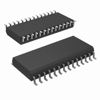
MCU 8BIT CMOS ROM OTP 28-SOIC
Manufacturer
National Semiconductor
Series
COP8™ 8SGr
Datasheet
1.COP8SGE728N8NOPB.pdf
(62 pages)
Specifications of COP8SGR728M7/NOPB
Core Processor
COP8
Core Size
8-Bit
Speed
15MHz
Connectivity
Microwire/Plus (SPI), UART/USART
Peripherals
POR, PWM, WDT
Number Of I /o
24
Program Memory Size
32KB (32K x 8)
Program Memory Type
OTP
Ram Size
512 x 8
Voltage - Supply (vcc/vdd)
2.7 V ~ 5.5 V
Oscillator Type
Internal
Operating Temperature
-40°C ~ 125°C
Package / Case
28-SOIC
Data Bus Width
8 bit
Maximum Clock Frequency
15 MHz
Data Ram Size
512 B
Number Of Programmable I/os
40
Number Of Timers
3
Height
2.34 mm
Interface Type
USART
Length
17.91 mm
Maximum Operating Temperature
+ 125 C
Minimum Operating Temperature
- 40 C
Supply Voltage (max)
5.5 V
Supply Voltage (min)
2.7 V
Width
7.49 mm
For Use With
COP8SG-EPU - BOARD PROTOTYPE/TARGET COP8
Lead Free Status / RoHS Status
Lead free / RoHS Compliant
Eeprom Size
-
Data Converters
-
Lead Free Status / Rohs Status
Details
Other names
COP8SGR728M7


AC Electrical Characteristics
Input Offset Voltage (Note 12)
Input Common Mode Voltage Range
Voltage Gain
Low Level Output Current
High Level Output Current
DC Supply Current per Comparator
(When Enabled)
Response Time (Note 13)
Comparator Enable Time(Note 14)
Note 4: Maximum rate of voltage change must be
Note 5: Supply and IDLE currents are measured with CKI driven with a square wave Oscillator, External Oscillator, inputs connected to V
but not connected to a load.
Note 6: The HALT mode will stop CKI from oscillating in the R/C and the Crystal configurations. In the R/C configuration, CKI is forced high internally. In the crystal
or external configuration, CKI is TRI-STATE. Measurement of I
programmed as low outputs and not driving a load; all outputs programmed low and not driving a load; all inputs tied to V
to HALT mode entered via setting bit 7 of the G Port data register.
Note 7: Pins G6 and RESET are designed with a high voltage input network. These pins allow input voltages
biased at voltages
pins will not latch up. The voltage at the pins must be limited to
ESD transients.
Note 8: National Semiconductor uses the High Temperature Storage Life (HTSL) test to evaluate the data retention capabilities of the EPROM memory cells used
in our OTP microcontrollers. Qualification devices have been stressed at 150˚C for 1000 hours. Under these conditions, our EPROM cells exhibit data retention
capabilities in excess of 29 years. This is based on an activation energy of 0.7eV derated to 55˚C.
Note 9: Parameter characterized but not tested.
Note 10: Rise times faster than the minimum specification may trigger an internal power-on-reset.
Note 11: MICROWIRE Setup and Hold Times and Propagation Delays are referenced to the appropriate edge of the MICROWIRE clock. See and the MICROWIRE
operation description.
Comparators AC and DC Characteristics
Note 12: The comparator inputs are high impedance port inputs and, as such, input current is limited to port input leakage current.
Note 13: Response time is measured from a step input to a valid logic level at the comparator output. software response time is dependent of instruction execution.
Note 14: Comparator enable time is that delay time required between the end of the instruction cycle that enables the comparator and using the output of the
comparator, either by hardware or by software.
V
CC
= 5V, −40˚C
Parameter
>
V
CC
(the pins do not have source current when biased at a voltage below V
T
A
+85˚C.
<
0.5 V/ms.
FIGURE 3. MICROWIRE/PLUS Timing
0.4V
V
V
200 mV step input
100 mV Overdrive,
100 pF Load
OL
OH
= 0.4V
= V
<
DD
(Continued)
14V. WARNING: Voltages in excess of 14V will cause damage to the pins. This warning excludes
Conditions
V
HALT is done with device neither sourcing nor sinking current; with L. F, C, G0, and G2–G5
CC
IN
− 0.4V
V
CC
− 1.5V
9
CC
−1.6
Min
0.4
1.6
). The effective resistance to V
10131709
>
V
CC
Typ
100
±
and the pins will have sink current to V
5
CC
; clock monitor disabled. Parameter refers
CC
V
CC
is 750
Max
±
150
600
600
CC
15
− 1.5
and outputs driven low
(typical). These two
www.national.com
CC
Units
mV
mA
mA
dB
µA
ns
ns
when
V
Related parts for COP8SGR728M7/NOPB
Image
Part Number
Description
Manufacturer
Datasheet
Request
R

Part Number:
Description:
National Semiconductor [8-Bit D/A Converter]
Manufacturer:
National Semiconductor
Datasheet:
Part Number:
Description:
National Semiconductor [Media Coprocessor]
Manufacturer:
National Semiconductor
Datasheet:
Part Number:
Description:
Digitally Controlled Tone and Volume Circuit with Stereo Audio Power Amplifier, Microphone Preamp Stage and National 3D Sound
Manufacturer:
National Semiconductor
Datasheet:
Part Number:
Description:
Digitally Controlled Tone and Volume Circuit with Stereo Audio Power Amplifier, Microphone Preamp Stage and National 3D Sound
Manufacturer:
National Semiconductor
Datasheet:
Part Number:
Description:
AC97 Rev 2 Codec with Sample Rate Conversion and National 3D Sound
Manufacturer:
National Semiconductor
Part Number:
Description:
Manufacturer:
National Semiconductor
Datasheet:
Part Number:
Description:
Manufacturer:
National Semiconductor
Datasheet:
Part Number:
Description:
General Purpose, Low Voltage, Low Power, Rail-to-Rail Output Operational Amplifiers
Manufacturer:
National Semiconductor
Datasheet:
Part Number:
Description:
8-bit 20 MSPS flash A/D converter.
Manufacturer:
National Semiconductor
Datasheet:
Part Number:
Description:
Low Noise Quad Operational Amplifier
Manufacturer:
National Semiconductor
Datasheet:
Part Number:
Description:
Quad Differential Line Receivers
Manufacturer:
National Semiconductor
Datasheet:
Part Number:
Description:
Quad High Speed Trapezoidal? Bus Transceiver
Manufacturer:
National Semiconductor
Datasheet:
Part Number:
Description:
Dual Line Receiver
Manufacturer:
National Semiconductor
Datasheet:
Part Number:
Description:
TTL to 10k ECL Level Translator with Latch
Manufacturer:
National Semiconductor
Datasheet: