COP8SGR728M7/NOPB National Semiconductor, COP8SGR728M7/NOPB Datasheet - Page 29
COP8SGR728M7/NOPB
Manufacturer Part Number
COP8SGR728M7/NOPB
Description
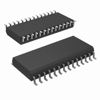
MCU 8BIT CMOS ROM OTP 28-SOIC
Manufacturer
National Semiconductor
Series
COP8™ 8SGr
Datasheet
1.COP8SGE728N8NOPB.pdf
(62 pages)
Specifications of COP8SGR728M7/NOPB
Core Processor
COP8
Core Size
8-Bit
Speed
15MHz
Connectivity
Microwire/Plus (SPI), UART/USART
Peripherals
POR, PWM, WDT
Number Of I /o
24
Program Memory Size
32KB (32K x 8)
Program Memory Type
OTP
Ram Size
512 x 8
Voltage - Supply (vcc/vdd)
2.7 V ~ 5.5 V
Oscillator Type
Internal
Operating Temperature
-40°C ~ 125°C
Package / Case
28-SOIC
Data Bus Width
8 bit
Maximum Clock Frequency
15 MHz
Data Ram Size
512 B
Number Of Programmable I/os
40
Number Of Timers
3
Height
2.34 mm
Interface Type
USART
Length
17.91 mm
Maximum Operating Temperature
+ 125 C
Minimum Operating Temperature
- 40 C
Supply Voltage (max)
5.5 V
Supply Voltage (min)
2.7 V
Width
7.49 mm
For Use With
COP8SG-EPU - BOARD PROTOTYPE/TARGET COP8
Lead Free Status / RoHS Status
Lead free / RoHS Compliant
Eeprom Size
-
Data Converters
-
Lead Free Status / Rohs Status
Details
Other names
COP8SGR728M7


8.0 USART
PEN: This bit enables/disables Parity (7- and 8-bit modes
only). Read/Write, cleared on reset.
PEN = 0
PEN = 1
PSEL1, PSEL0: Parity select bits. Read/Write, cleared on
reset.
PSEL1 = 0, PSEL0 = 0
PSEL1 = 0, PSEL0 = 1
PSEL1 = 1, PSEL0 = 0
PSEL1 = 1, PSEL0 = 1
XBIT9/PSEL0: Programs the ninth bit for transmission when
the USART is operating with nine data bits per frame. For
seven or eight data bits per frame, this bit in conjunction with
PSEL1 selects parity. Read/Write, cleared on reset.
CHL1, CHL0: These bits select the character frame format.
Parity is not included and is generated/verified by hardware.
Read/Write, cleared on reset.
CHL1 = 0, CHL0 = 0
CHL1 = 0, CHL0 = 1
CHL1 = 1, CHL0 = 0
CHL1 = 1, CHL0 = 1
ERR: This bit is a global USART error flag which gets set if
any or a combination of the errors (DOE, FE, PE) occur.
Read only; it cannot be written by software, cleared on reset.
RBFL: This bit is set when the USART has received a
complete character and has copied it into the RBUF register.
It is automatically reset when software reads the character
from RBUF. Read only; it cannot be written by software,
cleared on reset.
TBMT: This bit is set when the USART transfers a byte of
data from the TBUF register into the TSFT register for trans-
mission. It is automatically reset when software writes into
the TBUF register. Read only, bit is set to “one” on reset; it
cannot be written by software.
ENUR-USART Receive Control and Status Register
(Address at 0BB)
Note 16: Bit is reserved for future use. User must set to zero.
DOE: Flags a Data Overrun Error. Read only, cleared on
read, cleared on reset.
DOE = 0
DOE = 1
FE: Flags a Framing Error. Read only, cleared on read,
cleared on reset.
FE = 0
FE = 1
PE: Flags a Parity Error. Read only, cleared on read, cleared
on reset.
PE = 0
Bit 7
DOE
FE
since the last time the ENUR register was read.
Indicates no Framing Error has been detected
Indicates the occurrence of a Framing Error.
Indicates no Parity Error has been detected since
Parity disabled.
Parity enabled.
Indicates no Data Overrun Error has been de-
tected since the last time the ENUR register
was read.
Indicates the occurrence of a Data Overrun
Error.
PE
Reserved
(Note 16)
(Continued)
The frame contains eight data bits.
The frame contains seven data bits.
The frame contains nine data bits.
Loopback Mode selected. Trans-
mitter output internally looped back
to receiver input. Nine bit framing
format is used.
Odd Parity (if Parity enabled)
Even Parity (if Parity enabled)
Mark(1) (if Parity enabled)
Space(0) (if Parity enabled)
RBIT9
ATTN
XMTG RCVG
Bit 0
29
PE = 1
SPARE: Reserved for future use. Read/Write, cleared on
reset.
RBIT9: Contains the ninth data bit received when the US-
ART is operating with nine data bits per frame. Read only,
cleared on reset.
ATTN: ATTENTION Mode is enabled while this bit is set.
This bit is cleared automatically on receiving a character with
data bit nine set. Read/Write, cleared on reset.
XMTG: This bit is set to indicate that the USART is transmit-
ting. It gets reset at the end of the last frame (end of last Stop
bit). Read only, cleared on reset.
RCVG: This bit is set high whenever a framing error occurs
and goes low when RDX goes high. Read only, cleared on
reset.
ENUI-USART Interrupt and Clock Source Register
(Address at 0BC)
STP2: This bit programs the number of Stop bits to be
transmitted. Read/Write, cleared on reset.
STP2 = 0
STP2 = 1
STP78: This bit is set to program the last Stop bit to be 7/8th
of a bit in length. Read/Write, cleared on reset.
ETDX: TDX (USART Transmit Pin) is the alternate function
assigned to Port L pin L2; it is selected by setting ETDX bit.
To simulate line break generation, software should reset
ETDX bit and output logic zero to TDX pin through Port L
data and configuration registers. Read/Write, cleared on
reset.
SSEL: USART mode select. Read/Write, cleared on reset.
SSEL = 0
SSEL = 1
XRCLK: This bit selects the clock source for the receiver
section. Read/Write, cleared on reset.
XRCLK = 0
XRCLK = 1
XTCLK: This bit selects the clock source for the transmitter
section. Read/Write, cleared on reset.
XTCLK = 0
XTCLK = 1
ERI: This bit enables/disables interrupt from the receiver
section. Read/Write, cleared on reset.
ERI = 0
ERI = 1
ETI: This bit enables/disables interrupt from the transmitter
section. Read/Write, cleared on reset.
ETI = 0
ETI = 1
Bit 7
STP2 STP78 ETDX
the last time the ENUR register was read.
Indicates the occurrence of a Parity Error.
Interrupt from the transmitter is disabled.
Interrupt from the transmitter is enabled.
Interrupt from the receiver is disabled.
Interrupt from the receiver is enabled.
One Stop bit transmitted.
Two Stop bits transmitted.
Asynchronous Mode.
Synchronous Mode.
The clock source is selected through the PSR
and BAUD registers.
Signal on CKX (L1) pin is used as the clock.
The clock source is selected through the
PSR and BAUD registers.
Signal on CKX (L1) pin is used as the clock.
SSEL XRCLK XTCLK
ERI
www.national.com
ETI
Bit 0
Related parts for COP8SGR728M7/NOPB
Image
Part Number
Description
Manufacturer
Datasheet
Request
R

Part Number:
Description:
National Semiconductor [8-Bit D/A Converter]
Manufacturer:
National Semiconductor
Datasheet:
Part Number:
Description:
National Semiconductor [Media Coprocessor]
Manufacturer:
National Semiconductor
Datasheet:
Part Number:
Description:
Digitally Controlled Tone and Volume Circuit with Stereo Audio Power Amplifier, Microphone Preamp Stage and National 3D Sound
Manufacturer:
National Semiconductor
Datasheet:
Part Number:
Description:
Digitally Controlled Tone and Volume Circuit with Stereo Audio Power Amplifier, Microphone Preamp Stage and National 3D Sound
Manufacturer:
National Semiconductor
Datasheet:
Part Number:
Description:
AC97 Rev 2 Codec with Sample Rate Conversion and National 3D Sound
Manufacturer:
National Semiconductor
Part Number:
Description:
Manufacturer:
National Semiconductor
Datasheet:
Part Number:
Description:
Manufacturer:
National Semiconductor
Datasheet:
Part Number:
Description:
General Purpose, Low Voltage, Low Power, Rail-to-Rail Output Operational Amplifiers
Manufacturer:
National Semiconductor
Datasheet:
Part Number:
Description:
8-bit 20 MSPS flash A/D converter.
Manufacturer:
National Semiconductor
Datasheet:
Part Number:
Description:
Low Noise Quad Operational Amplifier
Manufacturer:
National Semiconductor
Datasheet:
Part Number:
Description:
Quad Differential Line Receivers
Manufacturer:
National Semiconductor
Datasheet:
Part Number:
Description:
Quad High Speed Trapezoidal? Bus Transceiver
Manufacturer:
National Semiconductor
Datasheet:
Part Number:
Description:
Dual Line Receiver
Manufacturer:
National Semiconductor
Datasheet:
Part Number:
Description:
TTL to 10k ECL Level Translator with Latch
Manufacturer:
National Semiconductor
Datasheet: