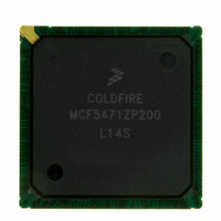
MCF5471ZP200 Freescale Semiconductor, MCF5471ZP200 Datasheet - Page 18

MCF5471ZP200
Manufacturer Part Number
MCF5471ZP200
Description
IC MPU 32BIT COLDF 388-PBGA
Manufacturer
Freescale Semiconductor
Series
MCF547xr
Datasheet
1.MCF5472VR200.pdf
(34 pages)
Specifications of MCF5471ZP200
Core Processor
Coldfire V4E
Core Size
32-Bit
Speed
200MHz
Connectivity
EBI/EMI, Ethernet, I²C, SPI, UART/USART, USB
Peripherals
DMA, PWM, WDT
Number Of I /o
99
Program Memory Type
ROMless
Ram Size
32K x 8
Voltage - Supply (vcc/vdd)
1.43 V ~ 1.58 V
Oscillator Type
External
Operating Temperature
0°C ~ 70°C
Package / Case
388-BGA
Family Name
MCF5xxx
Device Core
ColdFire V4e
Device Core Size
32b
Frequency (max)
200MHz
Instruction Set Architecture
RISC
Supply Voltage 1 (typ)
1.5/3.3V
Operating Supply Voltage (max)
1.58/3.6V
Operating Supply Voltage (min)
1.43/3V
Operating Temp Range
0C to 70C
Operating Temperature Classification
Commercial
Mounting
Surface Mount
Pin Count
388
Package Type
BGA
For Use With
M5475EVBGHS - KIT DEV GHS FOR M5475EVBM5474GFE - MODULE M5474 FIRE ENGINEM5474LITEKIT - KIT DEV FOR MCF547X
Lead Free Status / RoHS Status
Contains lead / RoHS non-compliant
Eeprom Size
-
Program Memory Size
-
Data Converters
-
Lead Free Status / Rohs Status
Not Compliant
Available stocks
Company
Part Number
Manufacturer
Quantity
Price
Company:
Part Number:
MCF5471ZP200
Manufacturer:
Freescale
Quantity:
92
Company:
Part Number:
MCF5471ZP200
Manufacturer:
MOTOLOLA
Quantity:
490
SDRAM Bus
9.2
When using the DDR SDRAM controller, the following timing numbers must be followed to properly latch or drive data onto
the memory bus. All timing numbers are relative to the four DQS byte lanes.
Table
18
Symbol
DD10
DD11
DD12
DD1
DD2
DD3
DD4
DD5
DD6
DD7
DD8
DD9
12shows the DDR clock crossover specifications.
1
Symbol
The clock crossover voltage is only guaranteed when using the highest drive strength option for the SDCLK[1:0]
and SDCLK[1:0] signals.
V
V
V
V
OUT
MP
DDR SDRAM AC Timing Characteristics
Frequency of Operation
Clock Period (t
Pulse Width High (t
Pulse Width Low (t
Address, SDCKE, CAS, RAS, WE, SDBA, SDCS—Output
Valid (t
Address, SDCKE, CAS, RAS, WE, SDBA, SDCS—Output Hold
(t
Write Command to first DQS Latching Transition (t
Data and Data Mask Output Setup (DQ−>DQS) Relative to
DQS (DDR Write Mode) (t
Data and Data Mask Output Hold (DQS−>DQ) Relative to DQS
(DDR Write Mode) (t
Input Data Skew Relative to DQS (Input Setup) (t
Input Data Hold Relative to DQS (t
DQS falling edge to SDCLK rising (output setup time) (t
DQS falling edge from SDCLK rising (output hold time) (t
ID
IX
SDCLK
SDCLK
CMH
)
Clock output mid-point voltage
Clock output voltage level
Clock output differential voltage (peak to peak swing)
Clock crossing point voltage
CMV
)
CK
)
CKL
CKH
QH
)
)
)
Characteristic
Table 12. DDR Clock Crossover Specifications
QS
Characteristic
MCF547x ColdFire
Figure 15. DDR Clock Timing Diagram
)
Table 13. DDR Timing Specifications
1
IH
)
®
IS
Microprocessor, Rev. 4
DQSS
)
)
DSS
DSH
)
)
0.25 × SDCLK
+ 0.5ns
7.52
0.45
0.45
Min
50
2.0
1.0
1.0
0.5
0.5
—
—
1.05
–0.3
1.05
Min
0.7
1
0.5 × SDCLK
SD_VDD + 0.3
SD_VDD + 0.6
+ 1.0 ns
Max
0.55
0.55
1.25
133
12
—
—
—
—
—
—
1
Max
1.45
1.45
V
V
V
Freescale Semiconductor
IX
MP
IX
V
SDCLK
SDCLK
SDCLK
ID
MHz
Unit
ns
ns
ns
ns
ns
ns
ns
ns
ns
Unit
V
V
V
V
Notes
10
11
2
3
4
5
6
7
8
9


