MCF5471ZP200 Freescale Semiconductor, MCF5471ZP200 Datasheet - Page 22
MCF5471ZP200
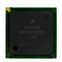
Manufacturer Part Number
MCF5471ZP200
Description
IC MPU 32BIT COLDF 388-PBGA
Manufacturer
Freescale Semiconductor
Series
MCF547xr
Datasheet
1.MCF5472VR200.pdf
(34 pages)
Specifications of MCF5471ZP200
Core Processor
Coldfire V4E
Core Size
32-Bit
Speed
200MHz
Connectivity
EBI/EMI, Ethernet, I²C, SPI, UART/USART, USB
Peripherals
DMA, PWM, WDT
Number Of I /o
99
Program Memory Type
ROMless
Ram Size
32K x 8
Voltage - Supply (vcc/vdd)
1.43 V ~ 1.58 V
Oscillator Type
External
Operating Temperature
0°C ~ 70°C
Package / Case
388-BGA
Family Name
MCF5xxx
Device Core
ColdFire V4e
Device Core Size
32b
Frequency (max)
200MHz
Instruction Set Architecture
RISC
Supply Voltage 1 (typ)
1.5/3.3V
Operating Supply Voltage (max)
1.58/3.6V
Operating Supply Voltage (min)
1.43/3V
Operating Temp Range
0C to 70C
Operating Temperature Classification
Commercial
Mounting
Surface Mount
Pin Count
388
Package Type
BGA
For Use With
M5475EVBGHS - KIT DEV GHS FOR M5475EVBM5474GFE - MODULE M5474 FIRE ENGINEM5474LITEKIT - KIT DEV FOR MCF547X
Lead Free Status / RoHS Status
Contains lead / RoHS non-compliant
Eeprom Size
-
Program Memory Size
-
Data Converters
-
Lead Free Status / Rohs Status
Not Compliant
Available stocks
Company
Part Number
Manufacturer
Quantity
Price
Company:

Part Number:
MCF5471ZP200
Manufacturer:
Freescale
Quantity:
92
Company:
Part Number:
MCF5471ZP200
Manufacturer:
MOTOLOLA
Quantity:
490


Fast Ethernet AC Timing Specifications
11
11.1
The following timing specs are defined at the chip I/O pin and must be translated appropriately to arrive at timing
specs/constraints for the EMAC_10_100 I/O signals.
The following timing specs meet the requirements for MII and 7-Wire style interfaces for a range of transceiver devices. If this
interface is to be used with a specific transceiver device the timing specs may be altered to match that specific transceiver.
22
1
2
3
4
5
6
Num
P10
P11
P12
Please see the reset configuration signals description in the “Signal Descriptions” chapter within the MCF547x
Reference Manual. Also specific guidelines may need to be followed when operating the system PLL below certain
frequencies.
Max cycle rate is determined by CLKIN and how the user has the system PLL configured.
All signals defined as PCI bused signals. Does not include PTP (point-to-point) signals.
PCI 2.2 spec does not require an output hold time. Although the MCF547X may provide a slight amount of hold, it
is not required or guaranteed.
PCI 2.2 spec requires zero input hold.
These signals are defined at PTP (Point-to-point) in the PCI 2.2 spec.
P7
P8
P9
Fast Ethernet AC Timing Specifications
MII/7-WIRE Interface Timing Specs
PCI GNT (0 < PCI ≤ 33Mhz) - Input Setup (t
PCI signals (0–66 Mhz) - Input Hold (t
PCI REQ/GNT (33 < PCI ≤ 66Mhz) - Output valid (t
PCI REQ/GNT (0 < PCI ≤ 33Mhz) - Output valid (t
PCI REQ/GNT (33 < PCI ≤ 66Mhz) - Input Setup (t
PCI REQ (0 < PCI ≤ 33Mhz) - Input Setup (t
Setup/Hold
Valid/Hold
Output
CLKIN
Input
Table 14. PCI Timing Specifications (continued)
MCF547x ColdFire
Characteristic
Figure 18. PCI Timing
P4
IH
)
P1
IS
IS
®
)
)
Microprocessor, Rev. 4
P2
Output Valid
DV
Input Valid
IS
DV
)
)
)
P6
P7
Min
—
—
—
12
10
0
Max
12
—
—
—
6
5
Freescale Semiconductor
Unit
ns
ns
ns
ns
ns
ns
Notes
5
6
Related parts for MCF5471ZP200
Image
Part Number
Description
Manufacturer
Datasheet
Request
R

Part Number:
Description:
Manufacturer:
Freescale Semiconductor, Inc
Datasheet:
Part Number:
Description:
Manufacturer:
Freescale Semiconductor, Inc
Datasheet:
Part Number:
Description:
Manufacturer:
Freescale Semiconductor, Inc
Datasheet:
Part Number:
Description:
Manufacturer:
Freescale Semiconductor, Inc
Datasheet:
Part Number:
Description:
Manufacturer:
Freescale Semiconductor, Inc
Datasheet:
Part Number:
Description:
Manufacturer:
Freescale Semiconductor, Inc
Datasheet:
Part Number:
Description:
Manufacturer:
Freescale Semiconductor, Inc
Datasheet:
Part Number:
Description:
Manufacturer:
Freescale Semiconductor, Inc
Datasheet:
Part Number:
Description:
Manufacturer:
Freescale Semiconductor, Inc
Datasheet:
Part Number:
Description:
Manufacturer:
Freescale Semiconductor, Inc
Datasheet:
Part Number:
Description:
Manufacturer:
Freescale Semiconductor, Inc
Datasheet:
Part Number:
Description:
Manufacturer:
Freescale Semiconductor, Inc
Datasheet:
Part Number:
Description:
Manufacturer:
Freescale Semiconductor, Inc
Datasheet:
Part Number:
Description:
Manufacturer:
Freescale Semiconductor, Inc
Datasheet:
Part Number:
Description:
Manufacturer:
Freescale Semiconductor, Inc
Datasheet: