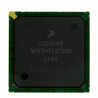
MCF5471ZP200 Freescale Semiconductor, MCF5471ZP200 Datasheet - Page 7

MCF5471ZP200
Manufacturer Part Number
MCF5471ZP200
Description
IC MPU 32BIT COLDF 388-PBGA
Manufacturer
Freescale Semiconductor
Series
MCF547xr
Datasheet
1.MCF5472VR200.pdf
(34 pages)
Specifications of MCF5471ZP200
Core Processor
Coldfire V4E
Core Size
32-Bit
Speed
200MHz
Connectivity
EBI/EMI, Ethernet, I²C, SPI, UART/USART, USB
Peripherals
DMA, PWM, WDT
Number Of I /o
99
Program Memory Type
ROMless
Ram Size
32K x 8
Voltage - Supply (vcc/vdd)
1.43 V ~ 1.58 V
Oscillator Type
External
Operating Temperature
0°C ~ 70°C
Package / Case
388-BGA
Family Name
MCF5xxx
Device Core
ColdFire V4e
Device Core Size
32b
Frequency (max)
200MHz
Instruction Set Architecture
RISC
Supply Voltage 1 (typ)
1.5/3.3V
Operating Supply Voltage (max)
1.58/3.6V
Operating Supply Voltage (min)
1.43/3V
Operating Temp Range
0C to 70C
Operating Temperature Classification
Commercial
Mounting
Surface Mount
Pin Count
388
Package Type
BGA
For Use With
M5475EVBGHS - KIT DEV GHS FOR M5475EVBM5474GFE - MODULE M5474 FIRE ENGINEM5474LITEKIT - KIT DEV FOR MCF547X
Lead Free Status / RoHS Status
Contains lead / RoHS non-compliant
Eeprom Size
-
Program Memory Size
-
Data Converters
-
Lead Free Status / Rohs Status
Not Compliant
Available stocks
Company
Part Number
Manufacturer
Quantity
Price
Company:
Part Number:
MCF5471ZP200
Manufacturer:
Freescale
Quantity:
92
Company:
Part Number:
MCF5471ZP200
Manufacturer:
MOTOLOLA
Quantity:
490
The relationship between SD V
3.3V) and EV
4.2.1
If EV
to the EV
must power up. IV
high current in the internal ESD protection diodes. The rise times on the power supplies should be slower than 1 microsecond
to avoid turning on the internal ESD protection clamp diodes.
The recommended power up sequence is as follows:
4.2.2
If IV
There is no limit on how long after IV
not lag EV
ESD protection diodes. There are no requirements for the fall times of the power supplies.
The recommended power down sequence is as follows:
Freescale Semiconductor
1.
2.
1.
2.
DD
DD
PLL V
/SD V
Use 1 microsecond or slower rise time for all supplies.
IV
V
Drop IV
Drop EV
DD
DD
DD
DD
/SD V
, SD V
DD
going to the higher external voltages. One way to accomplish this is to use a low drop-out voltage regulator.
Power Up Sequence
Power Down Sequence
/PLL V
DD
DD
are specified relative to IV
DD
are powered down first, sense circuits in the I/O pads cause all output drivers to be in a high impedance state.
are powered up with the IV
DD
DD
DD
DD
/PLL V
/SD V
to be in a high impedance state. There is no limit to how long after EV
3.3V
2.5V
1.5V
DD
should not lead the EV
, or PLL V
NOTES:
0
and EV
Figure 3. Supply Voltage Sequencing and Separation Cautions
DD
DD
1.
2.
3.
4.
supplies
IVDD should not exceed EVDD or SD VDD by more than 0.4V
at any time, including power-up.
Recommended that IVDD/PLL VDD should track EVDD/SD VDD up to
0.9V, then separate for completion of ramps.
Input voltage must not be greater than the supply voltage (EVDD, SD VDD,
IVDD, or PLL VDD) by more than 0.5V at any time, including during power-up.
Use 1 microsecond or slower rise time for all supplies.
to 0V
DD
DD
DD
and EV
/SD V
1
going low by more than 0.4V during power down or there is undesired high current in the
DD
MCF547x ColdFire
and PLL V
DD
2
DD
DD
DD
DD
should track up to 0.9V, then separate for the completion of ramps with EV
is non-critical during power-up and power-down sequences. SD V
.
, SD V
at 0V, the sense circuits in the I/O pads cause all pad output drivers connected
DD
Supplies Stable
DD
power down before EV
, or PLL V
®
Microprocessor, Rev. 4
DD
by more than 0.4V during power ramp up or there is
DD
or SD V
EV
SD V
IV
DD
DD
DD
DD
Hardware Design Considerations
, PLL V
DD
, SD V
/SD V
must power down. IV
(2.5V)
DD
DD
DD
Time
(3.3V)
powers up before IV
DD
DD
(2.5V or
DD
should
/SD
DD
7


