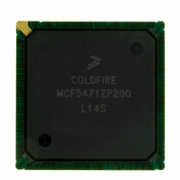
MCF5471ZP200 Freescale Semiconductor, MCF5471ZP200 Datasheet - Page 8

MCF5471ZP200
Manufacturer Part Number
MCF5471ZP200
Description
IC MPU 32BIT COLDF 388-PBGA
Manufacturer
Freescale Semiconductor
Series
MCF547xr
Datasheet
1.MCF5472VR200.pdf
(34 pages)
Specifications of MCF5471ZP200
Core Processor
Coldfire V4E
Core Size
32-Bit
Speed
200MHz
Connectivity
EBI/EMI, Ethernet, I²C, SPI, UART/USART, USB
Peripherals
DMA, PWM, WDT
Number Of I /o
99
Program Memory Type
ROMless
Ram Size
32K x 8
Voltage - Supply (vcc/vdd)
1.43 V ~ 1.58 V
Oscillator Type
External
Operating Temperature
0°C ~ 70°C
Package / Case
388-BGA
Family Name
MCF5xxx
Device Core
ColdFire V4e
Device Core Size
32b
Frequency (max)
200MHz
Instruction Set Architecture
RISC
Supply Voltage 1 (typ)
1.5/3.3V
Operating Supply Voltage (max)
1.58/3.6V
Operating Supply Voltage (min)
1.43/3V
Operating Temp Range
0C to 70C
Operating Temperature Classification
Commercial
Mounting
Surface Mount
Pin Count
388
Package Type
BGA
For Use With
M5475EVBGHS - KIT DEV GHS FOR M5475EVBM5474GFE - MODULE M5474 FIRE ENGINEM5474LITEKIT - KIT DEV FOR MCF547X
Lead Free Status / RoHS Status
Contains lead / RoHS non-compliant
Eeprom Size
-
Program Memory Size
-
Data Converters
-
Lead Free Status / Rohs Status
Not Compliant
Available stocks
Company
Part Number
Manufacturer
Quantity
Price
Company:
Part Number:
MCF5471ZP200
Manufacturer:
Freescale
Quantity:
92
Company:
Part Number:
MCF5471ZP200
Manufacturer:
MOTOLOLA
Quantity:
490
Hardware Design Considerations
4.3
4.3.1
4.3.2
Connecting the USBVBUS pin directly to the 5V VBUS signal from the USB connector can cause long-term reliability
problems in the ESD network of the processor. Therefore, use of an external voltage divider for VBUS is recommended.
Figure 4
should connect. Point B, marked in each figure, is where a 3.3V version of VBUS should connect to the USBVBUS pin on the
device.
4.3.3
It is recommended to connect the shield and the ground pin of the B USB receptacle for upstream ports to the board ground
plane. The ground pin of the A USB receptacles for downstream ports should also be connected to the board ground plane, but
industry practice varies widely on the connection of the shield of the A USB receptacles to other system grounds. Take
precautions for control of ground loops between hosts and self-powered USB devices through the cable shield.
8
1.
2.
3.
4.
5.
6.
7.
8.
9.
High speed clock and the USBD+ and USBD- differential pair should be routed first.
Route USBD+ and USBD- signals on the top layer of the board.
The trace width and spacing of the USBD+ and USBD- signals should be such that the differential impedance is 90Ω.
Route traces over continuous planes (power and ground)—they should not pass over any power/ground plane slots or
anti-etch. When placing connectors, make sure the ground plane clear-outs around each pin have ground continuity
between all pins.
Maintain the parallelism (skew matched) between USBD+ and USBD-. These traces should be the same overall length.
Do not route USBD+ and USBD- traces under oscillators or parallel to clock traces and/or data buses. Minimize the
lengths of high speed signals that run parallel to the USBD+ and USBD- pair. Maintain a minimum 50mil spacing to
clock signals.
Keep USBD+ and USBD- traces as short as possible.
Route USBD+, USBD-, and USBVBUS signals with a minimum amount of vias and corners. Use 45° turns.
Stubs should be avoided as much as possible. If they cannot be avoided, stubs should be no greater than 200mils.
and
General USB Layout Guidelines
Figure 5
USB D+ and D- High-Speed Traces
USB VBUS Traces
USB Receptacle Connections
depict possible connections for VBUS. Point A, marked in each figure, is where a 5V version of VBUS
(5V)
(5V)
MCF547x ColdFire
Figure 4. Preferred VBUS Connections
Figure 5. Alternate VBUS Connections
A
A
8.2k
50k
20k
(3.3V)
(3.3V)
B
B
®
Microprocessor, Rev. 4
50k
50k
MCF547x
MCF547x
50k
50k
Freescale Semiconductor


