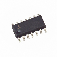
X40420S14I-B Intersil, X40420S14I-B Datasheet - Page 11

X40420S14I-B
Manufacturer Part Number
X40420S14I-B
Description
IC VOLT MON DUAL SUP/SW 14-SOIC
Manufacturer
Intersil
Type
Multi-Voltage Supervisorr
Datasheet
1.X40420S14Z-B.pdf
(25 pages)
Specifications of X40420S14I-B
Number Of Voltages Monitored
2
Output
Open Drain, Open Drain
Reset
Active High/Active Low
Reset Timeout
Adjustable/Selectable
Voltage - Threshold
2.6V, 4.6V
Operating Temperature
-40°C ~ 85°C
Mounting Type
Surface Mount
Package / Case
14-SOIC (3.9mm Width), 14-SOL
Lead Free Status / RoHS Status
Contains lead / RoHS non-compliant
Available stocks
Company
Part Number
Manufacturer
Quantity
Price
Company:
Part Number:
X40420S14I-B
Manufacturer:
Intersil
Quantity:
100
Figure 8. Valid Start and Stop Conditions
Serial Acknowledge
Acknowledge is a software convention used to indi-
cate successful data transfer. The transmitting device,
either master or slave, will release the bus after trans-
mitting eight bits. During the ninth clock cycle, the
receiver will pull the SDA line LOW to acknowledge
that it received the eight bits of data. See Figure 9.
The device will respond with an acknowledge after
recognition of a start condition and if the correct
Device Identifier and Select bits are contained in the
Slave Address Byte. If a write operation is selected,
the device will respond with an acknowledge after the
receipt of each subsequent eight bit word. The device
will acknowledge all incoming data and address bytes,
except for the Slave Address Byte when the Device
Identifier and/or Select bits are incorrect.
In the read mode, the device will transmit eight bits of
data, release the SDA line, then monitor the line for an
acknowledge. If an acknowledge is detected and no
stop condition is generated by the master, the device
will continue to transmit data. The device will terminate
further data transmissions if an acknowledge is not
Figure 9. Acknowledge Response From Receiver
from Receiver
Data Output
Data Output
SCL from
Master
from
SDA
SCL
11
Start
Start
1
X40420, X40421
detected. The master must then issue a stop condition
to return the device to Standby mode and place the
device into a known state.
Serial Write Operations
Byte Write
For a write operation, the device requires the Slave
Address Byte and a Word Address Byte. This gives
the master access to any one of the words in the
array. After receipt of the Word Address Byte, the
device responds with an acknowledge, and awaits the
next eight bits of data. After receiving the 8 bits of the
Data Byte, the device again responds with an
acknowledge. The master then terminates the transfer
by generating a stop condition, at which time the
device begins the internal write cycle to the nonvolatile
memory. During this internal write cycle, the device
inputs are disabled, so the device will not respond to any
requests from the master. The SDA output is at high
impedance. See Figure 12.
A write to a protected block of memory will suppress
the acknowledge bit.
8
Stop
Acknowledge
9
May 25, 2006


