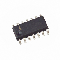
X40420S14I-B Intersil, X40420S14I-B Datasheet - Page 16

X40420S14I-B
Manufacturer Part Number
X40420S14I-B
Description
IC VOLT MON DUAL SUP/SW 14-SOIC
Manufacturer
Intersil
Type
Multi-Voltage Supervisorr
Datasheet
1.X40420S14Z-B.pdf
(25 pages)
Specifications of X40420S14I-B
Number Of Voltages Monitored
2
Output
Open Drain, Open Drain
Reset
Active High/Active Low
Reset Timeout
Adjustable/Selectable
Voltage - Threshold
2.6V, 4.6V
Operating Temperature
-40°C ~ 85°C
Mounting Type
Surface Mount
Package / Case
14-SOIC (3.9mm Width), 14-SOL
Lead Free Status / RoHS Status
Contains lead / RoHS non-compliant
Available stocks
Company
Part Number
Manufacturer
Quantity
Price
Company:
Part Number:
X40420S14I-B
Manufacturer:
Intersil
Quantity:
100
ABSOLUTE MAXIMUM RATINGS
Temperature under bias .................... -65°C to +135°C
Storage temperature ......................... -65°C to +150°C
Voltage on any pin with
D.C. output current ............................................... 5mA
Lead temperature (soldering, 10s) .................... 300°C
D.C. OPERATING CHARACTERISTICS
(Over the recommended operating conditions unless otherwise specified)
I
BATT1
RECOMMENDED OPERATING CONDITIONS
Symbol
I
I
I
V
V
respect to V
SB1
SB2
BATT2
V
I
I
OUT1
OUT2
V
CC1
CC2
V
V
V
BSH
I
OHB
IH
OLB
I
IL
LO
LI
Temperature
(1)(7)
(2)(7)
(3)
(3)
Commercial
(3)(7)
(1)
(1)
(7)
(7)
(7)
(7)
Industrial
Active Supply Current (
(Excludes I
Active Supply Current (
Volatile Memory (Excludes I
Standby Current (
Standby Current (
V
V
(Battery Backup Mode)
Output Voltage (V
V
Output Voltage (V
V
Output (BATT-ON) LOW Voltage
Output (BATT-ON) HIGH Voltage
Battery Switch Hysteresis
(V
Input Leakage Current (SCL, MR, WP)
Output Leakage Current (SDA, V2FAIL,
WDO, RESET)
Input LOW Voltage (SDA, SCL, MR, WP)
Input HIGH Voltage (SDA, SCL, MR, WP)
BATT
BATT
CC
CC
SS
CC
...................................... -1.0V to +7V
> V
< V
< V
Current (Excludes I
Current (Excludes I
TRIP1
TRIP1
TRIP1
OUT
)
) {Battery Backup}
)
16
)
Parameter
V
V
-40°C
Min.
CC
CC
0°C
CC
CC
> V
< V
) AC (WDT off)
) DC (WDT on)
V
V
BATT
BATT
CC
CC
OUT
OUT
) Read
) Write Non
OUT
)
)
– 0.03V and
+ 0.03V or
)
+85°C
Max.
70°C
X40420, X40421
V
V
V
V
V
CC
BATT
CC
CC
OUT
Min.
-0.5
-0.05V
-0.5V
x 0.7
*See ordering Info
-0.8
-0.2
Version Chip Supply Voltage
-A or -B
COMMENT
Stresses above those listed under “Absolute Maximum
Ratings” may cause permanent damage to the device.
This is a stress rating only; functional operation of the
device (at these or any other conditions above those
listed in the operational sections of this specification) is
not implied. Exposure to absolute maximum rating con-
ditions for extended periods may affect device reliability.
-C
Typ.
-30
0.4
25
30
6
(5)
V
V
CC
CC
2.7V to 5.5V
2.7V to 5.5V
Max.
1.5
3.0
0.4
30
10
10
10
1
6
+ 0.5
x 0.3
Unit
mA
mA
mV
µA
µA
µA
µA
µA
µA
V
V
V
V
V
V
V
V
f
V
VIH =
f
V
Others = GND or
V
V
V
I
I
I
I
I
Power-up
Power-down
V
V
Device is in Standby
SCL
SCL
OUT
OUT
OUT
OL
OH
IL
IH
IL
SDA
OUT
BATT
OUT
IL
SDA
Test Conditions
=
=
= 3.0mA (4.5-5.5V)
= GND to
=
= -0.4mA (4.5-5.5V)
, f
= 400kHz
= 5mA (4.5-5.5V)
= 50mA (4.5-5.5V)
= 250µA
V
V
= V
=
=
= GND to
V
SDA
V
1.6V to 3.6V
=
Monitored
CC
CC
Voltages*
2.6 to 5.5V
CC
V
Open
CC
2.8V
SCL
CC
= 400kHz
x 0.1
x 0.1
x 0.9,
x 0.9
=
V
V
CC
V
May 25, 2006
CC
CC
V
CC
(2)


