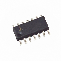
X40420S14I-B Intersil, X40420S14I-B Datasheet - Page 9

X40420S14I-B
Manufacturer Part Number
X40420S14I-B
Description
IC VOLT MON DUAL SUP/SW 14-SOIC
Manufacturer
Intersil
Type
Multi-Voltage Supervisorr
Datasheet
1.X40420S14Z-B.pdf
(25 pages)
Specifications of X40420S14I-B
Number Of Voltages Monitored
2
Output
Open Drain, Open Drain
Reset
Active High/Active Low
Reset Timeout
Adjustable/Selectable
Voltage - Threshold
2.6V, 4.6V
Operating Temperature
-40°C ~ 85°C
Mounting Type
Surface Mount
Package / Case
14-SOIC (3.9mm Width), 14-SOL
Lead Free Status / RoHS Status
Contains lead / RoHS non-compliant
Available stocks
Company
Part Number
Manufacturer
Quantity
Price
Company:
Part Number:
X40420S14I-B
Manufacturer:
Intersil
Quantity:
100
BP: Block Protect Bit (Nonvolatile)
The Block Protect Bits BP determines which blocks of
the array are write protected. A write to a protected
block of memory is ignored. The block protect bit will
prevent write operations to half the array segment.
PUP1, PUP0: Power-uppower-up Bits (Nonvolatile)
The Power-up bits, PUP1 and PUP0, determine the
t
shown in the following table.
WD1, WD0: Watchdog Timer Bits
The bits WD1 and WD0 control the period of the
Watchdog Timer. The options are shown below.
Writing to the Control Registers
Changing any of the nonvolatile bits of the control and
trickle registers requires the following steps:
– Write a 02H to the Control Register to set the Write
– Write a 06H to the Control Register to set the
PURST
PUP1
0
1
WD1
Enable Latch (WEL). This is a volatile operation, so
there is no delay after the write. (Operation pre-
ceded by a start and ended with a stop).
Register Write Enable Latch (RWEL) and the WEL
bit. This is also a volatile cycle. The zeros in the data
byte are required. (Operation proceeded by a start
and ended with a stop).
0
0
1
1
0
0
1
1
100h – 1FFh (256 bytes)
Protected Addresses
time delay. The nominal power-up times are
PUP0
WD0
0
1
0
1
0
1
0
1
(Size)
None
Power-on Reset Delay (
Watchdog Time Out Period
disabled (factory default)
9
200 milliseconds
200ms (default)
25 milliseconds
1.4 seconds
400ms
800ms
50ms
Memory Array
Upper Half of
Array Lock
Memory
None
t
PURST
X40420, X40421
)
– Write a one byte value to the Control Register that
– A read operation occurring between any of the previ-
– The RWEL bit cannot be reset without writing to the
To illustrate, a sequence of writes to the device con-
sisting of [02H, 06H, 02H] will reset all of the nonvola-
tile bits in the Control Register to 0. A sequence of
[02H, 06H, 06H] will leave the nonvolatile bits
unchanged and the RWEL bit remains set.
Note: 1. t
Fault Detection Register (FDR)
The Fault Detection Register provides the user the
status of what causes the system reset active. The
Manual Reset Fail, Watchdog Timer Fail and Three
Low Voltage Fail bits are volatile
The FDR is accessed with a special preamble in the
slave byte (1011) and is located at address 0FFh. It
can only be modified by performing a byte write opera-
tion directly to the address of the register and only one
data byte is allowed for each register write operation.
There is no need to set the WEL or RWEL in the con-
trol register to access this fault detection register.
LV1F
has all the control bits set to the desired state. The
Control register can be represented as qxys 001r in
binary, where xy are the WD bits, and st are the BP
bits and qr are the power-up bits. This operation pro-
ceeded by a start and ended with a stop bit. Since
this is a nonvolatile write cycle it will take up to 10ms
to complete. The RWEL bit is reset by this cycle and
the sequence must be repeated to change the non-
volatile bits again. If bit 2 is set to ‘1’ in this third step
(qxys 011r) then the RWEL bit is set, but the WD1,
WD0, PUP1, PUP0, and BP bits remain unchanged.
Writing a second byte to the control register is not
allowed. Doing so aborts the write operation and
returns a NACK.
ous operations will not interrupt the register write
operation.
nonvolatile control bits in the control register, power
cycling the device or attempting a write to a write
protected block.
7
2. Watchdog timer bits are shipped disabled.
LV2F
PURST
6
is set to 200ms as factory default.
5
0
WDF
4
MRF
3
2
0
1
0
May 25, 2006
0
0


