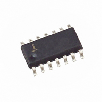
X40420S14I-B Intersil, X40420S14I-B Datasheet - Page 14

X40420S14I-B
Manufacturer Part Number
X40420S14I-B
Description
IC VOLT MON DUAL SUP/SW 14-SOIC
Manufacturer
Intersil
Type
Multi-Voltage Supervisorr
Datasheet
1.X40420S14Z-B.pdf
(25 pages)
Specifications of X40420S14I-B
Number Of Voltages Monitored
2
Output
Open Drain, Open Drain
Reset
Active High/Active Low
Reset Timeout
Adjustable/Selectable
Voltage - Threshold
2.6V, 4.6V
Operating Temperature
-40°C ~ 85°C
Mounting Type
Surface Mount
Package / Case
14-SOIC (3.9mm Width), 14-SOL
Lead Free Status / RoHS Status
Contains lead / RoHS non-compliant
Available stocks
Company
Part Number
Manufacturer
Quantity
Price
Company:
Part Number:
X40420S14I-B
Manufacturer:
Intersil
Quantity:
100
A similar operation called “Set Current Address” where
the device will perform this operation if a stop is issued
instead of the second start is shown in Figure 15. The
device will go into standby mode after the stop and all
bus activity will be ignored until a start is detected.
This operation loads the new address into the address
counter. The next Current Address Read operation will
read from the newly loaded address. This operation
could be useful if the master knows the next address it
needs to read, but is not ready for the data.
Sequential Read
Sequential reads can be initiated as either a current
address read or random address read. The first Data
Byte is transmitted as with the other modes; however,
the master now responds with an acknowledge, indicat-
ing it requires additional data. The device continues to
output data for each acknowledge received. The master
terminates the read operation by not responding with an
acknowledge and then issuing a stop condition.
The data output is sequential, with the data from
address n followed by the data from address n + 1. The
address counter for read operations increments through
all page and column addresses, allowing the entire
memory contents to be serially read during one opera-
tion. At the end of the address space the counter “rolls
over” to address 0000
put data for each acknowledge received. See Figure 17
for the acknowledge and data transfer sequence.
Figure 14. Current Address Read Sequence
H
and the device continues to out-
14
Signals from
Signals from
the Master
the Slave
SDA Bus
S
a
t
r
t
1 0 1
X40420, X40421
Address
Slave
0
0
1
SERIAL DEVICE ADDRESSING
Memory Address Map
CR, Control Register, CR7: CR0
Address: 1FF
FDR, Fault DetectionRegister, FDR7: FDR0
Address: 0FF
General Purpose Memory Organization, A8:A0
Address: 00h to 1FFh
General Purpose Memory Array Configuration
Slave Address Byte
Following a start condition, the master must output a
Slave Address Byte. This byte consists of several parts:
– a device type identifier that is always “1010” when
– two bits of “0”.
– one bit that becomes the MSB of the memory
– last bit of the slave command byte is a R/W bit. The
A
C
K
Memory Address
accessing the array and “1011” when accessing the
control register and fault detection register.
address X
R/W bit of the Slave Address Byte defines the oper-
ation to be performed. When the R/W bit is a one,
then a read operation is selected. A zero selects a
write operation. See Figure 16.
Data
A8:A0
0FFh
1FFh
000h
100h
4
.
hex
hex
Lower 256 bytes
Upper 256 bytes
S
o
p
t
Block Protect Option
May 25, 2006


