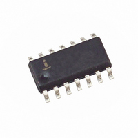
X40420S14I-B Intersil, X40420S14I-B Datasheet - Page 15

X40420S14I-B
Manufacturer Part Number
X40420S14I-B
Description
IC VOLT MON DUAL SUP/SW 14-SOIC
Manufacturer
Intersil
Type
Multi-Voltage Supervisorr
Datasheet
1.X40420S14Z-B.pdf
(25 pages)
Specifications of X40420S14I-B
Number Of Voltages Monitored
2
Output
Open Drain, Open Drain
Reset
Active High/Active Low
Reset Timeout
Adjustable/Selectable
Voltage - Threshold
2.6V, 4.6V
Operating Temperature
-40°C ~ 85°C
Mounting Type
Surface Mount
Package / Case
14-SOIC (3.9mm Width), 14-SOL
Lead Free Status / RoHS Status
Contains lead / RoHS non-compliant
Available stocks
Company
Part Number
Manufacturer
Quantity
Price
Company:
Part Number:
X40420S14I-B
Manufacturer:
Intersil
Quantity:
100
Figure 15. Random Address Read Sequence
Figure 16. X40410/11 Addressing
Word Address
The word address is either supplied by the master or
obtained from an internal counter.
Operational Notes
The device powers-up in the following state:
– The device is in the low power standby state.
– The WEL bit is set to ‘0’. In this state it is not possi-
– SDA pin is the input mode.
– RESET/RESET Signal is active for
Figure 17. Sequential Read Sequence
General Purpose Memory
Control Register
Fault Detection Register
General Purpose Memory
Control Register
Fault Detection Register
ble to write to the device.
Signals from
Signals from
the Master
the Slave
SDA Bus
Signals from
Signals from
the Master
the Slave
SDA Bus
Word Address
Slave Byte
A7
1
1
1
1
1
15
Address
A6 A5 A4
Slave
0
0
0
1
1
S
a
t
r
t
1
1 0 1
1
1
1
1
1
A
C
K
Address
0
1
1
Slave
1
1
t
0
PURST
0
0
0
A3 A2
0
1
1
Data
(1)
0
0
0
0
.
1
1
A
C
K
A8 R/W
1
0
A1 A0
1
1
X40420, X40421
R/W
R/W
Address
C
A
K
1
1
Byte
Data
(2)
A
C
K
Data Protection
The following circuitry has been included to prevent
inadvertent writes:
– The WEL bit must be set to allow write operations.
– The proper clock count and bit sequence is required
– A three step sequence is required before writing into
– The WP pin, when held HIGH, prevents all writes to
S
a
t
r
t
prior to the stop bit in order to start a nonvolatile
write cycle.
the Control Register to change Watchdog Timer or
Block Lock settings.
the array and all the Register.
Address
A
C
K
Slave
(n is any integer greater than 1)
Data
(n-1)
1
C
A
K
Data
C
A
K
Data
(n)
S
o
p
t
S
o
p
t
May 25, 2006


