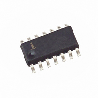
X40420S14I-B Intersil, X40420S14I-B Datasheet - Page 7

X40420S14I-B
Manufacturer Part Number
X40420S14I-B
Description
IC VOLT MON DUAL SUP/SW 14-SOIC
Manufacturer
Intersil
Type
Multi-Voltage Supervisorr
Datasheet
1.X40420S14Z-B.pdf
(25 pages)
Specifications of X40420S14I-B
Number Of Voltages Monitored
2
Output
Open Drain, Open Drain
Reset
Active High/Active Low
Reset Timeout
Adjustable/Selectable
Voltage - Threshold
2.6V, 4.6V
Operating Temperature
-40°C ~ 85°C
Mounting Type
Surface Mount
Package / Case
14-SOIC (3.9mm Width), 14-SOL
Lead Free Status / RoHS Status
Contains lead / RoHS non-compliant
Available stocks
Company
Part Number
Manufacturer
Quantity
Price
Company:
Part Number:
X40420S14I-B
Manufacturer:
Intersil
Quantity:
100
Resetting the V
To reset a V
age (Vp) to the WDO pin before a START condition is set
up on SDA. Next, issue on the SDA pin the Slave
Address A0h followed by the Byte Address 03h for
V
Byte in order to reset V
valid write operation initiates the programming sequence.
Pin WDO must then be brought LOW to complete the
operation.
After being reset, the value of V
value of 1.7V or lesser.
Note: This operation does not corrupt the memory array.
System Battery Switch
As long as V
V
switch. When the V
is applied to V
V
(typical) switch. V
RAM voltage, so the switchover circuit operates to pro-
tect the contents of the static RAM during a power failure.
Typically, when V
lower power state and draw much less current than in
their active mode. When V
back to V
a 60mV hysteresis around this battery switch threshold to
prevent oscillations between supplies.
While V
pulled LOW. The signal can drive an external PNP tran-
sistor to provide additional current to the external circuits
during normal operation.
Operation
The device is in normal operation with V
V
when V
Figure 5. Sample V
0.03V, then V
TRIP1
TRIP
BATT
CC
V
Adj.
> V
TRIP1
, V
- 0.03V. When V
and 0Bh for V
CC
CC
OUT
TRIP1
CC
goes away.
is connected to V
CC
when V
TRIPx
is connected to V
OUT
. It switches to the battery backup mode
OUT
exceeds the low voltage detect threshold
TRIPx
OUT
CC
is connected to V
voltage, apply the programming volt-
CC
if V
CC
TRIP
TRIP2
V
Voltage
typically supplies the system static
has failed, the SRAMs go into a
has fallen below V1
Adj.
CC
TRIP2
exceeds V
TRIPx
CC
Reset Circuit
, followed by 00h for the Data
is or equal to or greater than
7
drops to less than V
CC
. The STOP bit following a
OUT
CC
TRIPx
returns, V
BATT
through a 5Ω (typical)
the BATT-ON pin is
BATT
V2FAIL
RESET
4.7K
becomes a nominal
+ 0.03V. There is
through an 80Ω
TRIP
CC
OUT
as long as
, then V
switches
X40420, X40421
BATT
CC
1
6
2
7
-
X40420
Control Register
The Control Register provides the user a mechanism for
changing the Block Lock and Watchdog Timer settings.
The Block Lock and Watchdog Timer bits are nonvolatile
and do not change when power is removed.
The Control Register is accessed with a special pream-
ble in the slave byte (1011) and is located at address
1FFh. It can only be modified by performing a byte write
operation directly to the address of the register and only
one data byte is allowed for each register write operation.
Prior to writing to the Control Register, the WEL and
RWEL bits must be set using a two step process, with
the whole sequence requiring 3 steps. See "Writing to
the Control Registers" on page 9.
The user must issue a stop, after sending this byte to
the register, to initiate the nonvolatile cycle that stores
WD1, WD0, PUP1, PUP0, and BP. The X40420 will not
acknowledge any data bytes written after the first byte
is entered.
The state of the Control Register can be read at any time
by performing a random read at address 01Fh, using the
special preamble. Only one byte is read by each register
read operation. The master should supply a stop condi-
tion to be consistent with the bus protocol, but a stop is
not required to end this operation.
RWEL: Register Write Enable Latch (Volatile)
The RWEL bit must be set to “1” prior to a write to the
Control Register.
13
14
PUP1 WD1 WD0
9
8
V
V
V
0 ≤ V
and V
CC
CC
BATT
7
Condition
> V
> V
CC
CC
= 0
TRIP1
TRIP1
≤ V
6
< V
TRIP1
BATT
&
5
Adjust
Run
Normal Operation
Normal Operation without battery
backup capability
Battery Backup mode; RESET
signal is asserted. No communica-
tion to the device is allowed.
BP
4
V
P
Mode of Operation
3
0
SCL
SDA
RWEL WEL PUP0
2
µC
1
May 25, 2006
0


