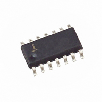
X40420S14I-B Intersil, X40420S14I-B Datasheet - Page 4

X40420S14I-B
Manufacturer Part Number
X40420S14I-B
Description
IC VOLT MON DUAL SUP/SW 14-SOIC
Manufacturer
Intersil
Type
Multi-Voltage Supervisorr
Datasheet
1.X40420S14Z-B.pdf
(25 pages)
Specifications of X40420S14I-B
Number Of Voltages Monitored
2
Output
Open Drain, Open Drain
Reset
Active High/Active Low
Reset Timeout
Adjustable/Selectable
Voltage - Threshold
2.6V, 4.6V
Operating Temperature
-40°C ~ 85°C
Mounting Type
Surface Mount
Package / Case
14-SOIC (3.9mm Width), 14-SOL
Lead Free Status / RoHS Status
Contains lead / RoHS non-compliant
Available stocks
Company
Part Number
Manufacturer
Quantity
Price
Company:
Part Number:
X40420S14I-B
Manufacturer:
Intersil
Quantity:
100
PIN DESCRIPTION
Pin
10
11
12
13
14
6
7
8
9
BATT-ON
RESET/
RESET
Name
V
V
SDA
SCL
V
V
WP
BATT
OUT
CC
SS
(Continued)
RESET Output. (X40421) This open drain pin is an active LOW output which goes LOW whenever
V
grammed time period (t
for t
RESET Output. (X40420) This pin is an active HIGH open drain output which goes HIGH whenever
V
grammed time period (t
for t
Ground
Serial Data. SDA is a bidirectional pin used to transfer data into and out of the device. It has an open
drain output and may be wire ORed with other open drain or open collector outputs. This pin requires
a pull up resistor and the input buffer is always active (not gated).
Watchdog Input. A HIGH to LOW transition on the SDA (while SCL is toggled from HIGH to LOW
and followed by a stop condition) restarts the Watchdog timer. The absence of this transition within
the watchdog time out period results in WDO going active.
Serial Clock. The Serial Clock controls the serial bus timing for data input and output.
Write Protect. WP HIGH prevents writes to any location in the device (including all the registers). It
has an internal pull down resistor. (>10MΩ typical)
Battery Supply Voltage. This input provides a backup supply in the event of a failure of the
primary V
maintain the contents of SRAM and also powers the internal logic to “stay awake.” If the battery is not
used, connect V
Output Voltage. (V)
IF V
Note: There is hysteresis around V
switchover voltage. A capacitance of 0.1µF must be connected to V
Battery On. This CMOS output goes HIGH when the V
V
requirements are greater than 50mA.
The purpose of this output is to drive an external transistor to get higher operating currents when the
V
pin and the external transistor is turned off. In this “backup condition,” the battery only needs to supply
enough voltage and current to keep SRAM devices from losing their data–there is no communication
at this time.
Supply Voltage
CC
CC
OUT
CC
V
then V
else V
PURST
PURST
CC
falls below V
falls below V
supply is fully functional. In the event of a V
OUT
switches to V
4
< V
CC
= V
OUT
OUT
thereafter.
thereafter.
TRIP1
voltage. The V
CC
= V
= V
BATT
if V
TRIP1
TRIP1
BATT
CC
CC
CC
. It is used to drive an external PNP pass transistor when V
to ground.
if V
> V
PURST
PURST
voltage or if manual reset is asserted. This output stays active for the pro-
voltage or if manual reset is asserted. This output stays active for the pro-
(ie if V
CC
TRIP1
BATT
> V
X40420, X40421
) on power-up. It will also stay active until manual reset is released and
) on power-up. It will also stay active until manual reset is released and
CC
BATT
.
voltage typically provides the supply voltage necessary to
< V
BATT
BATT
+ 0.03V
± 0.03V point to avoid oscillation at or near the
- 0.03V)
Function
CC
failure, the battery voltage is applied to the V
OUT
switches to V
OUT
to ensure stability.
BATT
CC
and goes LOW when
= V
OUT
and current
May 25, 2006
OUT


