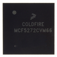
MCF5272CVM66 Freescale Semiconductor, MCF5272CVM66 Datasheet - Page 306

MCF5272CVM66
Manufacturer Part Number
MCF5272CVM66
Description
IC MPU 66MHZ COLDFIRE 196-MAPBGA
Manufacturer
Freescale Semiconductor
Series
MCF527xr
Specifications of MCF5272CVM66
Core Processor
Coldfire V2
Core Size
32-Bit
Speed
66MHz
Connectivity
EBI/EMI, Ethernet, I²C, SPI, UART/USART, USB
Peripherals
DMA, WDT
Number Of I /o
32
Program Memory Size
16KB (4K x 32)
Program Memory Type
ROM
Ram Size
1K x 32
Voltage - Supply (vcc/vdd)
3 V ~ 3.6 V
Oscillator Type
External
Operating Temperature
-40°C ~ 85°C
Package / Case
196-MAPBGA
Cpu Speed
66MHz
Embedded Interface Type
UART, QSPI, USB, TDM
Digital Ic Case Style
BGA
No. Of Pins
196
Supply Voltage Range
3V To 3.6V
Rohs Compliant
Yes
Family Name
MCF5xxx
Device Core
ColdFire
Device Core Size
32b
Frequency (max)
66MHz
Instruction Set Architecture
RISC
Supply Voltage 1 (typ)
3.3V
Operating Temp Range
-40C to 85C
Operating Temperature Classification
Industrial
Mounting
Surface Mount
Pin Count
196
Package Type
MA-BGA
Lead Free Status / RoHS Status
Lead free / RoHS Compliant
Eeprom Size
-
Data Converters
-
Lead Free Status / Rohs Status
Compliant
Available stocks
Company
Part Number
Manufacturer
Quantity
Price
Company:
Part Number:
MCF5272CVM66
Manufacturer:
MOT
Quantity:
3
Company:
Part Number:
MCF5272CVM66
Manufacturer:
Freescale Semiconductor
Quantity:
10 000
Part Number:
MCF5272CVM66
Manufacturer:
FREESCALE
Quantity:
20 000
Company:
Part Number:
MCF5272CVM66J
Manufacturer:
NSC
Quantity:
36
Company:
Part Number:
MCF5272CVM66J
Manufacturer:
Freescale Semiconductor
Quantity:
10 000
- Current page: 306 of 544
- Download datasheet (7Mb)
Physical Layer Interface Controller (PLIC)
Note that only the active, that is enabled, B- and D-channel receive and transmit registers need to be read
and written. B and D channels which are not active need not have their receive and transmit registers read
and written.
It should be clear from
frame (n) is written to the PLIC transmit register during the interrupt service routine of the previous frame,
frame (n-1). Similarly on the receive side, frame (n) is read from the PLIC receive register during the
interrupt service routine of the following frame, frame (n + 2).
delay through the PLIC, when not in loopback mode, is two 2-KHz frames, or 1 mS.
13.2.5.2
The aperiodic status interrupt is an interrupt which is driven by a number of conditions. The CPU services
this interrupt by reading the aperiodic status register, ASR, and by reading or writing the relevant C/I or
monitor channel register or registers which have generated this interrupt. Once read, the interrupt is
cleared. Each port and individual interrupts within each port is maskable. The following conditions for
each of the ports can trigger this interrupt:
13-10
•
•
•
•
Slot 0
125 μs
2-KHz interrupt
Monitor channel receive: ASR defines which port or ports have generated a monitor channel
receive interrupt. The interrupt service routine must then read the appropriate GMR register or
registers to clear the monitor channel receive interrupt.
Monitor channel transmit: ASR defines which port or ports have generated a monitor channel
transmit interrupt. The interrupt service routine must then read the appropriate GMT register or
registers to clear the monitor channel transmit interrupt.
C/I channel receive: ASR defines which port or ports have generated a C/I channel receive
interrupt. The interrupt service routine must then read the appropriate GCIR register or registers to
clear the C/I channel receive interrupt.
C/I channel transmit: ASR defines which port or ports have generated a C/I channel transmit
interrupt. The interrupt service routine must then read the appropriate GCIT register or registers to
clear the C/I channel transmit interrupt.
Read Frame n -1 (B&D)
Write Frame n + 1 (B&D)
Interrupt service routine
GCI Aperiodic Status Interrupt
Slot 1
Frame n
500 μs
MCF5272 ColdFire
Figure 13-10
Slot 2
Slot 3
Figure 13-10. Periodic Frame Interrupt
that due to the double buffering through the PLIC shadow register,
®
Integrated Microprocessor User’s Manual, Rev. 3
2-KHz interrupt
Slot 0
Interrupt service routine
Read Frame n (B&D)
Write Frame n + 2 (B&D)
Slot 1
Frame n + 1
Slot 2
Figure 13-10
Slot 3
2-KHz interrupt
Slot 0
shows that the minimum
Interrupt service routine
Read Frame n + 1 (B&D)
Write Frame n + 3 (B&D)
Frame n + 2
Slot 1
Freescale Semiconductor
Slot 2
Related parts for MCF5272CVM66
Image
Part Number
Description
Manufacturer
Datasheet
Request
R
Part Number:
Description:
Mcf5272 Coldfire Integrated Microprocessor User
Manufacturer:
Freescale Semiconductor, Inc
Datasheet:

Part Number:
Description:
MCF5272 Interrupt Service Routine for the Physical Layer Interface Controller
Manufacturer:
Freescale Semiconductor / Motorola
Datasheet:
Part Number:
Description:
Manufacturer:
Freescale Semiconductor, Inc
Datasheet:
Part Number:
Description:
Manufacturer:
Freescale Semiconductor, Inc
Datasheet:
Part Number:
Description:
Manufacturer:
Freescale Semiconductor, Inc
Datasheet:
Part Number:
Description:
Manufacturer:
Freescale Semiconductor, Inc
Datasheet:
Part Number:
Description:
Manufacturer:
Freescale Semiconductor, Inc
Datasheet:
Part Number:
Description:
Manufacturer:
Freescale Semiconductor, Inc
Datasheet:
Part Number:
Description:
Manufacturer:
Freescale Semiconductor, Inc
Datasheet:
Part Number:
Description:
Manufacturer:
Freescale Semiconductor, Inc
Datasheet:
Part Number:
Description:
Manufacturer:
Freescale Semiconductor, Inc
Datasheet:
Part Number:
Description:
Manufacturer:
Freescale Semiconductor, Inc
Datasheet:
Part Number:
Description:
Manufacturer:
Freescale Semiconductor, Inc
Datasheet:
Part Number:
Description:
Manufacturer:
Freescale Semiconductor, Inc
Datasheet:
Part Number:
Description:
Manufacturer:
Freescale Semiconductor, Inc
Datasheet:


