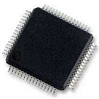
UPD78F0535GB(T)-UEU-A NEC, UPD78F0535GB(T)-UEU-A Datasheet - Page 206

UPD78F0535GB(T)-UEU-A
Manufacturer Part Number
UPD78F0535GB(T)-UEU-A
Description
8BIT MCU, 60K FLASH, 3KB RAM, LQFP
Manufacturer
NEC
Datasheet
1.UPD78F0535GBT-UEU-A.pdf
(773 pages)
Specifications of UPD78F0535GB(T)-UEU-A
Controller Family/series
UPD78
No. Of I/o's
55
Ram Memory Size
3KB
Cpu Speed
20MHz
No. Of Timers
8
No. Of Pwm
RoHS Compliant
Core Size
8bit
Program Memory Size
60KB
Oscillator Type
External, Internal
- Current page: 206 of 773
- Download datasheet (6Mb)
<R>
7.4.4 Operation in clear & start mode entered by TI00n pin valid edge input
start mode entered by the TI00n pin valid edge input) and the count clock (set by PRM0n) is supplied to the
timer/event counter, TM0n starts counting up. When the valid edge of the TI00n pin is detected during the counting
operation, TM0n is cleared to 0000H and starts counting up again. If the valid edge of the TI00n pin is not detected,
TM0n overflows and continues counting.
the start of the operation.
(1) Operation in clear & start mode entered by TI00n pin valid edge input
206
When bits 3 and 2 (TMC0n3 and TMC0n2) of 16-bit timer mode control register 0n (TMC0n) are set to 10 (clear &
The valid edge of the TI00n pin is a cause to clear TM0n. Starting the counter is not controlled immediately after
CR00n and CR01n are used as compare registers and capture registers.
Remarks 1. For the setting of the I/O pins, see 7.3 (5) Port mode register 0 (PM0).
(a) When CR00n and CR01n are used as compare registers
(b) When CR00n and CR01n are used as capture registers
Caution Do not set the count clock as the valid edge of the TI00n pin (PRM0n1 and PRM0n0 = 11). When
(CR00n: compare register, CR01n: compare register)
Remark n = 0:
Signals INTTM00n and INTTM01n are generated when the value of TM0n matches the value of CR00n and
CR01n.
The count value of TM0n is captured to CR00n and the INTTM00n signal is generated when the valid edge is
input to the TI01n pin (or when the phase reverse to that of the valid edge is input to the TI00n pin).
When the valid edge is input to the TI00n pin, the count value of TM0n is captured to CR01n and the
INTTM01n signal is generated. As soon as the count value has been captured, the counter is cleared to
0000H.
Count clock
TI00n pin
Figure 7-27. Block Diagram of Clear & Start Mode Entered by TI00n Pin Valid Edge Input
PRM0n1 and PRM0n0 = 11, TM0n is cleared.
2. For how to enable the INTTM00n signal interrupt, see CHAPTER 19 INTERRUPT FUNCTIONS.
n = 0, 1:
TMC0n3, TMC0n2
Operable bits
µ
µ
PD78F0531, 78F0532, 78F0533
PD78F0534, 78F0535, 78F0536, 78F0537, 78F0537D
(CR00n: Compare Register, CR01n: Compare Register)
detection
CHAPTER 7 16-BIT TIMER/EVENT COUNTERS 00 AND 01
Edge
Compare register
Timer counter
User’s Manual U17260EJ6V0UD
Match signal
(CR01n)
(TM0n)
Compare register
Clear
(CR00n)
Match signal
controller
Output
TO0n output
Interrupt signal
(INTTM00n)
Interrupt signal
(INTTM01n)
TO0n pin
Related parts for UPD78F0535GB(T)-UEU-A
Image
Part Number
Description
Manufacturer
Datasheet
Request
R

Part Number:
Description:
16/8 bit single-chip microcomputer
Manufacturer:
NEC
Datasheet:

Part Number:
Description:
Dual audio power amp circuit
Manufacturer:
NEC
Datasheet:

Part Number:
Description:
Dual comparator
Manufacturer:
NEC
Datasheet:

Part Number:
Description:
MOS type composite field effect transistor
Manufacturer:
NEC
Datasheet:

Part Number:
Description:
50 V/100 mA FET array incorporating 2 N-ch MOSFETs
Manufacturer:
NEC
Datasheet:

Part Number:
Description:
6-pin small MM high-frequency double transistor
Manufacturer:
NEC
Datasheet:

Part Number:
Description:
6-pin small MM high-frequency double transistor
Manufacturer:
NEC
Datasheet:

Part Number:
Description:
6-pin small MM high-frequency double transistor
Manufacturer:
NEC
Datasheet:

Part Number:
Description:
6-pin small MM high-frequency double transistor
Manufacturer:
NEC
Datasheet:

Part Number:
Description:
Twin transistors equipped with different model chips(6P small MM)
Manufacturer:
NEC
Datasheet:

Part Number:
Description:
Bipolar analog integrated circuit
Manufacturer:
NEC
Datasheet:


