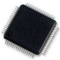
UPD78F0535GB(T)-UEU-A NEC, UPD78F0535GB(T)-UEU-A Datasheet - Page 638

UPD78F0535GB(T)-UEU-A
Manufacturer Part Number
UPD78F0535GB(T)-UEU-A
Description
8BIT MCU, 60K FLASH, 3KB RAM, LQFP
Manufacturer
NEC
Datasheet
1.UPD78F0535GBT-UEU-A.pdf
(773 pages)
Specifications of UPD78F0535GB(T)-UEU-A
Controller Family/series
UPD78
No. Of I/o's
55
Ram Memory Size
3KB
Cpu Speed
20MHz
No. Of Timers
8
No. Of Pwm
RoHS Compliant
Core Size
8bit
Program Memory Size
60KB
Oscillator Type
External, Internal
- Current page: 638 of 773
- Download datasheet (6Mb)
DC Characteristics (1/4)
(T
Notes 1. Value of current at which the device operation is guaranteed even if the current flows from V
Remark Unless specified otherwise, the characteristics of alternate-function pins are the same as those of port pins.
638
Output current, high
Output current, low
A
= −40 to +85°C, 1.8 V ≤ V
2. Value of current at which the device operation is guaranteed even if the current flows from an output pin to
3. Specification under conditions where the duty factor is 70% (time for which current is output is 0.7 × t and
Parameter
pin.
GND.
time for which current is not output is 0.3 × t, where t is a specific time). The total output current of the pins
at a duty factor of other than 70% can be calculated by the following expression.
• Where the duty factor of I
However, the current that is allowed to flow into one pin does not vary depending on the duty factor. A
current higher than the absolute maximum rating must not flow into one pin.
<Example> Where the duty factor is 50%, I
Note 2
Note 1
CHAPTER 30 ELECTRICAL SPECIFICATIONS ((A) GRADE PRODUCTS)
Total output current of pins = (20.0 × 0.7)/(50 × 0.01) = 28.0 mA
I
I
I
I
Symbol
OH1
OH2
OL1
OL2
DD
= EV
Per pin for P00 to P06, P10 to
P17, P30 to P33, P40 to P43,
P50 to P53, P70 to P77, P120,
P130, P140, P141
Total of P00 to P04, P40 to P43,
P120, P130, P140, P141
Total of P05, P06, P10 to P17,
P30 to P33, P50 to P53, P70 to
P77
Total
Per pin for P20 to P27
Per pin for P121 to P124
Per pin for P00 to P06, P10 to
P17, P30 to P33, P40 to P43,
P50 to P53, P70 to P77, P120,
P130, P140, P141
Per pin for P60 to P63
Total of P00 to P04, P40 to P43,
P120, P130, P140, P141
Total of P05, P06, P10 to P17,
P30 to P33, P50 to P53, P60 to
P63, P70 to P77
Total of all pins
Per pin for P20 to P27
Per pin for P121 to P124
DD
OH
Note 3
Note 3
≤ 5.5 V, AV
is n%: Total output current of pins = (I
of all pins
User’s Manual U17260EJ6V0UD
Note 3
Note 3
REF
Conditions
≤ V
OH
Note 3
Note 3
= 20.0 mA
DD
, V
SS
= EV
4.0 V ≤ V
2.7 V ≤ V
1.8 V ≤ V
4.0 V ≤ V
2.7 V ≤ V
1.8 V ≤ V
4.0 V ≤ V
2.7 V ≤ V
1.8 V ≤ V
4.0 V ≤ V
2.7 V ≤ V
1.8 V ≤ V
AV
4.0 V ≤ V
2.7 V ≤ V
1.8 V ≤ V
4.0 V ≤ V
2.7 V ≤ V
1.8 V ≤ V
4.0 V ≤ V
2.7 V ≤ V
1.8 V ≤ V
4.0 V ≤ V
2.7 V ≤ V
1.8 V ≤ V
4.0 V ≤ V
2.7 V ≤ V
1.8 V ≤ V
AV
REF
REF
SS
= V
= V
= AV
DD
DD
DD
DD
DD
DD
DD
DD
DD
DD
DD
DD
DD
DD
DD
DD
DD
DD
DD
DD
DD
DD
DD
DD
DD
DD
DD
DD
DD
≤ 5.5 V
< 4.0 V
< 2.7 V
≤ 5.5 V
< 4.0 V
< 2.7 V
≤ 5.5 V
< 4.0 V
< 2.7 V
≤ 5.5 V
< 4.0 V
< 2.7 V
≤ 5.5 V
< 4.0 V
< 2.7 V
≤ 5.5 V
< 4.0 V
< 2.7 V
≤ 5.5 V
< 4.0 V
< 2.7 V
≤ 5.5 V
< 4.0 V
< 2.7 V
≤ 5.5 V
< 4.0 V
< 2.7 V
OH
SS
× 0.7)/(n × 0.01)
= 0 V)
MIN.
TYP.
(A) grade products
DD
MAX.
−12.0
−18.0
−15.0
−10.0
−23.0
−20.0
−15.0
−3.0
−2.5
−1.0
−7.0
−5.0
−0.1
−0.1
15.0
20.0
15.0
45.0
35.0
20.0
65.0
50.0
29.0
8.5
5.0
2.0
5.0
2.0
9.0
0.4
0.4
to an output
Unit
mA
mA
mA
mA
mA
mA
mA
mA
mA
mA
mA
mA
mA
mA
mA
mA
mA
mA
mA
mA
mA
mA
mA
mA
mA
mA
mA
mA
mA
mA
mA
Related parts for UPD78F0535GB(T)-UEU-A
Image
Part Number
Description
Manufacturer
Datasheet
Request
R

Part Number:
Description:
16/8 bit single-chip microcomputer
Manufacturer:
NEC
Datasheet:

Part Number:
Description:
Dual audio power amp circuit
Manufacturer:
NEC
Datasheet:

Part Number:
Description:
Dual comparator
Manufacturer:
NEC
Datasheet:

Part Number:
Description:
MOS type composite field effect transistor
Manufacturer:
NEC
Datasheet:

Part Number:
Description:
50 V/100 mA FET array incorporating 2 N-ch MOSFETs
Manufacturer:
NEC
Datasheet:

Part Number:
Description:
6-pin small MM high-frequency double transistor
Manufacturer:
NEC
Datasheet:

Part Number:
Description:
6-pin small MM high-frequency double transistor
Manufacturer:
NEC
Datasheet:

Part Number:
Description:
6-pin small MM high-frequency double transistor
Manufacturer:
NEC
Datasheet:

Part Number:
Description:
6-pin small MM high-frequency double transistor
Manufacturer:
NEC
Datasheet:

Part Number:
Description:
Twin transistors equipped with different model chips(6P small MM)
Manufacturer:
NEC
Datasheet:

Part Number:
Description:
Bipolar analog integrated circuit
Manufacturer:
NEC
Datasheet:


