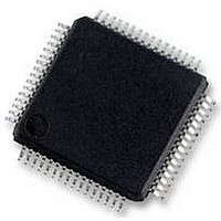
UPD78F0535GB(T)-UEU-A NEC, UPD78F0535GB(T)-UEU-A Datasheet - Page 741

UPD78F0535GB(T)-UEU-A
Manufacturer Part Number
UPD78F0535GB(T)-UEU-A
Description
8BIT MCU, 60K FLASH, 3KB RAM, LQFP
Manufacturer
NEC
Datasheet
1.UPD78F0535GBT-UEU-A.pdf
(773 pages)
Specifications of UPD78F0535GB(T)-UEU-A
Controller Family/series
UPD78
No. Of I/o's
55
Ram Memory Size
3KB
Cpu Speed
20MHz
No. Of Timers
8
No. Of Pwm
RoHS Compliant
Core Size
8bit
Program Memory Size
60KB
Oscillator Type
External, Internal
- Current page: 741 of 773
- Download datasheet (6Mb)
Serial
interface
UART6
Function
ASIM6:
Asynchronous
serial interface
operation mode
register 6
ASIS6:
Asynchronous
serial interface
reception error
status register 6
ASIF6:
Asynchronous
serial interface
transmission
status register 6 To initialize the transmission unit upon completion of continuous transmission, be
CKSR6: Clock
selection
register 6
BRGC6: Baud
rate generator
control register 6 The baud rate is the output clock of the 8-bit counter divided by 2.
ASICL6:
Asynchronous
serial interface
control register 6
Details of
Function
To start the transmission, set POWER6 to 1 and then set TXE6 to 1. To stop the
transmission, clear TXE6 to 0, and then clear POWER6 to 0.
To start the reception, set POWER6 to 1 and then set RXE6 to 1. To stop the
reception, clear RXE6 to 0, and then clear POWER6 to 0.
Set POWER6 to 1 and then set RXE6 to 1 while a high level is input to the R
pin. If POWER6 is set to 1 and RXE6 is set to 1 while a low level is input, reception
is started.
TXE6 and RXE6 are synchronized by the base clock (f
enable transmission or reception again, set TXE6 or RXE6 to 1 at least two clocks
of the base clock after TXE6 or RXE6 has been cleared to 0. If TXE6 or RXE6 is
set within two clocks of the base clock, the transmission circuit or reception circuit
may not be initialized.
Set transmit data to TXB6 at least one base clock (f
Clear the TXE6 and RXE6 bits to 0 before rewriting the PS61, PS60, and CL6 bits.
Fix the PS61 and PS60 bits to 0 when used in LIN communication operation.
Clear TXE6 to 0 before rewriting the SL6 bit. Reception is always performed with
“the number of stop bits = 1”, and therefore, is not affected by the set value of the
SL6 bit.
Make sure that RXE6 = 0 when rewriting the ISRM6 bit.
The operation of the PE6 bit differs depending on the set values of the PS61 and
PS60 bits of asynchronous serial interface operation mode register 6 (ASIM6).
For the stop bit of receive data, only the first stop bit is checked regardless of the
number of stop bits.
If an overrun error occurs, the next receive data is not written to receive buffer
register 6 (RXB6) but discarded.
If data is read from ASIS6, a wait cycle is generated. Do not read data from ASIS6
when the CPU is operating on the subsystem clock and the peripheral hardware
clock is stopped. For details, see CHAPTER 35 CAUTIONS FOR WAIT.
To transmit data continuously, write the first transmit data (first byte) to the TXB6
register. Be sure to check that the TXBF6 flag is “0”. If so, write the next transmit
data (second byte) to the TXB6 register. If data is written to the TXB6 register while
the TXBF6 flag is “1”, the transmit data cannot be guaranteed.
sure to check that the TXSF6 flag is “0” after generation of the transmission
completion interrupt, and then execute initialization. If initialization is executed while
the TXSF6 flag is “1”, the transmit data cannot be guaranteed.
Make sure POWER6 = 0 when rewriting TPS63 to TPS60.
Make sure that bit 6 (TXE6) and bit 5 (RXE6) of the ASIM6 register = 0 when
rewriting the MDL67 to MDL60 bits.
ASICL6 can be refreshed (the same value is written) by software during a
communication operation (when bits 7 and 6 (POWER6, TXE6) of ASIM6 = 1 or bits
7 and 5 (POWER6, RXE6) of ASIM6 = 1). However, do not set both SBRT6 and
SBTT6 to 1 by a refresh operation during SBF reception (SBRT6 = 1) or SBF
transmission (until INTST6 occurs since SBTT6 has been set (1)), because it may
re-trigger SBF reception or SBF transmission.
In the case of an SBF reception error, the mode returns to the SBF reception mode.
The status of the SBRF6 flag is held (1).
Before setting the SBRT6 bit, make sure that bit 7 (POWER6) and bit 5 (RXE6) of
ASIM6 = 1. After setting the SBRT6 bit to 1, do not clear it to 0 before SBF
reception is completed (before an interrupt request signal is generated).
APPENDIX D LIST OF CAUTIONS
User’s Manual U17260EJ6V0UD
Cautions
XCLK6
XCLK6
) after setting TXE6 = 1.
) set by CKSR6. To
X
D6
p. 363
p. 363
p. 363
p. 363
p. 363
p. 363
p. 363
p. 363
p. 363
p. 364
p. 364
p. 364
p. 364
p. 365
p. 365
p. 366
p. 367
p. 367
p. 368
p. 369
p. 369
(15/25)
Page
741
Related parts for UPD78F0535GB(T)-UEU-A
Image
Part Number
Description
Manufacturer
Datasheet
Request
R

Part Number:
Description:
16/8 bit single-chip microcomputer
Manufacturer:
NEC
Datasheet:

Part Number:
Description:
Dual audio power amp circuit
Manufacturer:
NEC
Datasheet:

Part Number:
Description:
Dual comparator
Manufacturer:
NEC
Datasheet:

Part Number:
Description:
MOS type composite field effect transistor
Manufacturer:
NEC
Datasheet:

Part Number:
Description:
50 V/100 mA FET array incorporating 2 N-ch MOSFETs
Manufacturer:
NEC
Datasheet:

Part Number:
Description:
6-pin small MM high-frequency double transistor
Manufacturer:
NEC
Datasheet:

Part Number:
Description:
6-pin small MM high-frequency double transistor
Manufacturer:
NEC
Datasheet:

Part Number:
Description:
6-pin small MM high-frequency double transistor
Manufacturer:
NEC
Datasheet:

Part Number:
Description:
6-pin small MM high-frequency double transistor
Manufacturer:
NEC
Datasheet:

Part Number:
Description:
Twin transistors equipped with different model chips(6P small MM)
Manufacturer:
NEC
Datasheet:

Part Number:
Description:
Bipolar analog integrated circuit
Manufacturer:
NEC
Datasheet:


