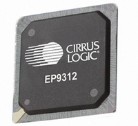
EP9312-CB Cirrus Logic Inc, EP9312-CB Datasheet - Page 527

EP9312-CB
Manufacturer Part Number
EP9312-CB
Description
System-on-Chip Processor
Manufacturer
Cirrus Logic Inc
Series
EP9r
Datasheets
1.EP9307-CRZ.pdf
(824 pages)
2.EP9312-IBZ.pdf
(4 pages)
3.EP9312-CB.pdf
(62 pages)
4.EP9312-CB.pdf
(17 pages)
Specifications of EP9312-CB
Peak Reflow Compatible (260 C)
No
A/d Converter
12 Bits
Leaded Process Compatible
No
No. Of I/o Pins
65
Package / Case
352-BGA
Core Processor
ARM9
Core Size
16/32-Bit
Speed
200MHz
Connectivity
EBI/EMI, EIDE, Ethernet, I²C, IrDA, Keypad/Touchscreen, SPI, UART/USART, USB
Peripherals
AC'97, DMA, I²:S, LCD, LED, MaverickKey, POR, PWM, WDT
Number Of I /o
16
Program Memory Type
ROMless
Ram Size
32K x 8
Voltage - Supply (vcc/vdd)
1.65 V ~ 3.6 V
Data Converters
A/D 8x12b
Oscillator Type
External
Operating Temperature
0°C ~ 70°C
Processor Series
EP93xx
Core
ARM920T
Data Bus Width
32 bit
3rd Party Development Tools
MDK-ARM, RL-ARM, ULINK2
Lead Free Status / RoHS Status
Contains lead / RoHS non-compliant
Eeprom Size
-
Program Memory Size
-
Lead Free Status / Rohs Status
No
Other names
598-1257
Available stocks
Company
Part Number
Manufacturer
Quantity
Price
Part Number:
EP9312-CB
Manufacturer:
CIRRUS
Quantity:
20 000
- EP9307-CRZ PDF datasheet
- EP9312-IBZ PDF datasheet #2
- EP9312-CB PDF datasheet #3
- EP9312-CB PDF datasheet #4
- Current page: 527 of 824
- Download datasheet (13Mb)
DS785UM1
14.2.1.10 Synchronizing Registers and Logic
14.2.2 UART Operation
The UART supports both asynchronous and synchronous operation of the clocks, PCLK and
UARTCLK. Synchronization registers and handshaking logic have been implemented, and
are active at all times. This has a minimal impact on performance or area. Synchronization of
control signals is performed on both directions of data flow, that is, from the PCLK to the
UARTCLK domain and from the UARTCLK domain to the PCLK.
Control data is written to the UART line control register, UARTLCR. This register is 23 bits
wide internally, but is externally accessed through the AMBA APB bus by three 8-bit wide
register locations, UARTLCR_H, UARTLCR_M and UARTLCR.L.
UARTLCR defines the baud rate divisor and transmission parameters, word length, buffer
mode, number of transmitted stop bits, parity mode and break generation.
The baud rate divisor is a 16-bit number used by the baud rate generator to determine the bit
period. The baud rate generator contains a 16-bit down counter, clocked by the UART
reference clock. When the value of the baud rate divisor has decremented to zero, the value
of the baud rate divisor is reloaded into the down counter, and an internal clock enable signal,
Baud16, is generated. This signal is then divided by 16 to give the transmit clock. A low
number in the baud rate divisor gives a short bit period and vice versa.
Data received or transmitted is stored in two 16-byte FIFOs, though the receive FIFO has an
extra three bits per character for status information.
For transmission, data is written into the transmit FIFO. This causes a data frame to start
transmitting with the parameters indicated in UARTLCR. Data continues to be transmitted
until there is no data left in the transmit FIFO. The BUSY signal goes HIGH as soon as data
is written to the transmit FIFO (that is, the FIFO is non-empty) and remains asserted HIGH
while data is being transmitted. BUSY is negated only when the transmit FIFO is empty, and
the last character has been transmitted from the shift register, including the stop bits. BUSY
can be asserted HIGH even though the UART may no longer be enabled.
When the receiver is idle (UARTRXD continuously 1, in the marking state) and a LOW is
detected on the data input (a start bit has been received), the receive counter, with the clock
enabled by Baud16, begins running and data is sampled on the eighth cycle of that counter
(half way through a bit period).
The start bit is valid if UARTRXD is still LOW on the eighth cycle of Baud16, otherwise a false
start bit is detected and it is ignored.
If the start bit was valid, successive data bits are sampled on every 16th cycle of Baud16 (that
is, one bit period later) according to the programmed length of the data characters. The parity
bit is then checked if parity mode was enabled.
Lastly, a valid stop bit is confirmed if UARTRXD is HIGH, otherwise a framing error has
occurred. When a full word has been received, the data is stored in the receive FIFO, with
any error bits associated with that word (see
Copyright 2007 Cirrus Logic
Table
14-1).
UART1 With HDLC and Modem Control Signals
EP93xx User’s Guide
14-5
14
Related parts for EP9312-CB
Image
Part Number
Description
Manufacturer
Datasheet
Request
R

Part Number:
Description:
IC ARM920T MCU 200MHZ 352-PBGA
Manufacturer:
Cirrus Logic Inc
Datasheet:

Part Number:
Description:
IC ARM9 SOC UNIVERSAL 352PBGA
Manufacturer:
Cirrus Logic Inc
Datasheet:

Part Number:
Description:
IC ARM920T MCU 200MHZ 352-PBGA
Manufacturer:
Cirrus Logic Inc
Datasheet:

Part Number:
Description:
IC Universal Platform ARM9 SOC Prcessor
Manufacturer:
Cirrus Logic Inc
Datasheet:

Part Number:
Description:
IC Universal Platform ARM9 SOC Prcessor
Manufacturer:
Cirrus Logic Inc
Datasheet:

Part Number:
Description:
Development Kit
Manufacturer:
Cirrus Logic Inc
Datasheet:

Part Number:
Description:
Development Kit
Manufacturer:
Cirrus Logic Inc
Datasheet:

Part Number:
Description:
High-efficiency PFC + Fluorescent Lamp Driver Reference Design
Manufacturer:
Cirrus Logic Inc
Datasheet:

Part Number:
Description:
Development Kit
Manufacturer:
Cirrus Logic Inc
Datasheet:

Part Number:
Description:
Development Kit
Manufacturer:
Cirrus Logic Inc
Datasheet:

Part Number:
Description:
Development Kit
Manufacturer:
Cirrus Logic Inc
Datasheet:

Part Number:
Description:
Development Kit
Manufacturer:
Cirrus Logic Inc
Datasheet:

Part Number:
Description:
Ref Bd For Speakerbar MSA & DSP Products
Manufacturer:
Cirrus Logic Inc


